
Semiconductor Foundry

Applied Materials and TSMC Collaborate at EPIC Center on Next-Generation Semiconductor Technologies for AI
Applied Materials announced a new innovation partnership with TSMC to develop materials, equipment, and process technologies for scaling next-generation semiconductor devices. The companies will work together at Applied’s EPIC Center in Silicon Valley. The partnership builds on more
6 min read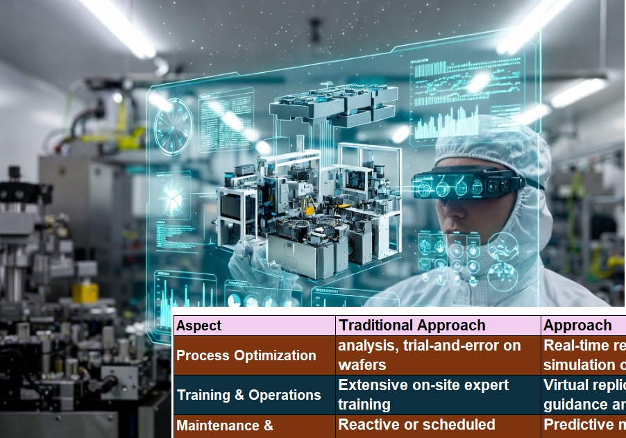
A Paradigm Shift in Semiconductor Manufacturing: The Power of Digital Twins and Virtual Fabs
Semiconductor chip fabs making chips in the nodes of 2nm and lower are among the most demanding manufacturing environments on earth. Producing advanced chips at scale requires sub-nanometer precision, ultraclean process conditions, hundreds of interdependent process steps, and workforces whose ex
10 min read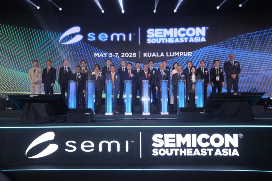
SEMICON Southeast Asia 2026 Opens in Kuala Lumpur with Focus on Advanced Packaging and Supply Chain Shifts
SEMICON Southeast Asia 2026 officially launched at the Malaysia International Trade and Exhibition Centre (MITEC). The event runs from 5 to 7 May under the theme ‘Transform Tomorrow’ and is held in strategic partnership with the Ministry of Investment, Trade and Industry (MITI) and th
5 min read
Karnataka Allocates 140 Acres to Applied Materials at Bengaluru Signature Business Park for ₹780 Crore
The Karnataka cabinet on April 30 approved the allotment of 140 acres of land at the Bengaluru Signature Business Park (BSBP), near Kempegowda International Airport, to US-based semiconductor equipment major Applied Materials Inc. for ₹780 crore. The land allocation was made on a lease-cum-s
1 min read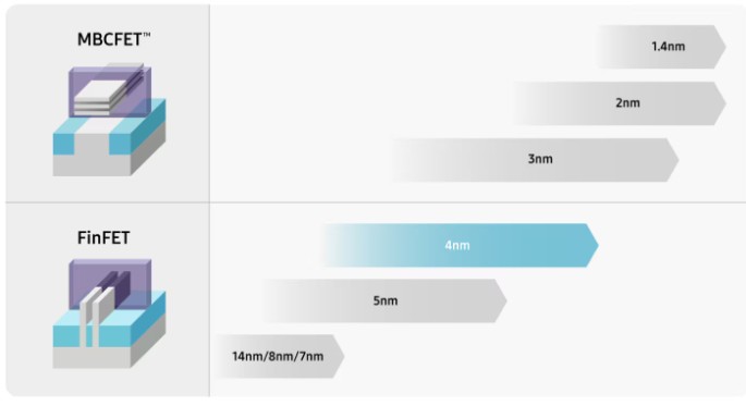
Samsung Pitches 4nm FinFET Foundry Process as Ideal “Sweet Spot” Between Mature and Cutting-Edge Nodes
Samsung Foundry is actively promoting its 4nm process technology as a practical midway solution for chip designers who want advanced performance without the extreme costs and risks of the latest 2nm nodes. In a new blog post on its semiconductor website, Samsung highlights the 4nm FinFET p
3 min read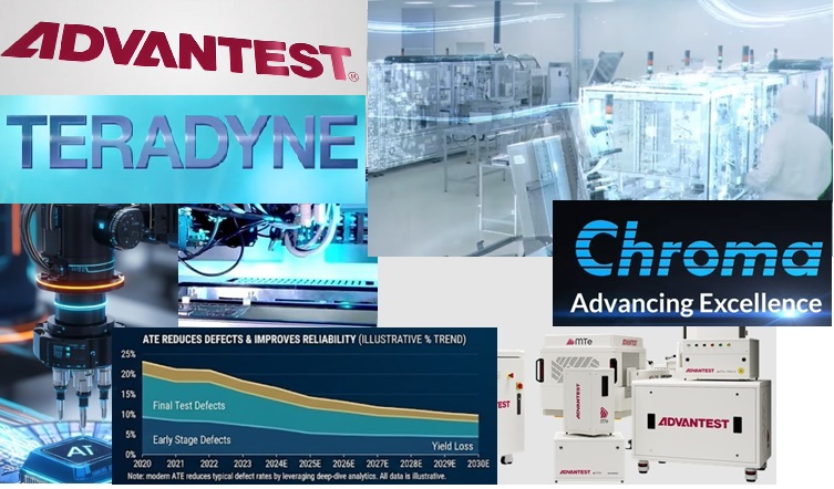
The Unsung Hero of AI Chips: How ATE is Revolutionizing Semiconductor Testing in the Intelligent Era
Innovation fuels semiconductor manufacturing, yet testing and quality assurance remain its unsung hero. While new features of advanced chip capture attention, device reliability and consistent performance under all operating conditions ultimately determine real-world success. Extreme automation a
9 min read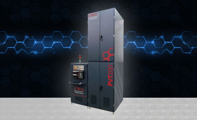
CVD Equipment Corporation Grows Single Crystal SiC Boules on PVT Systems with Stony Brook University
Semiconductor Equipment maker CVD Equipment announced the successful growth of single crystal silicon carbide (SiC) boules using its Physical Vapor Transport (PVT) Systems. The boules were characterized by Stony Brook University (SBU) as part of the new onsemi Research Center for Wide Bandgap Mat
2 min read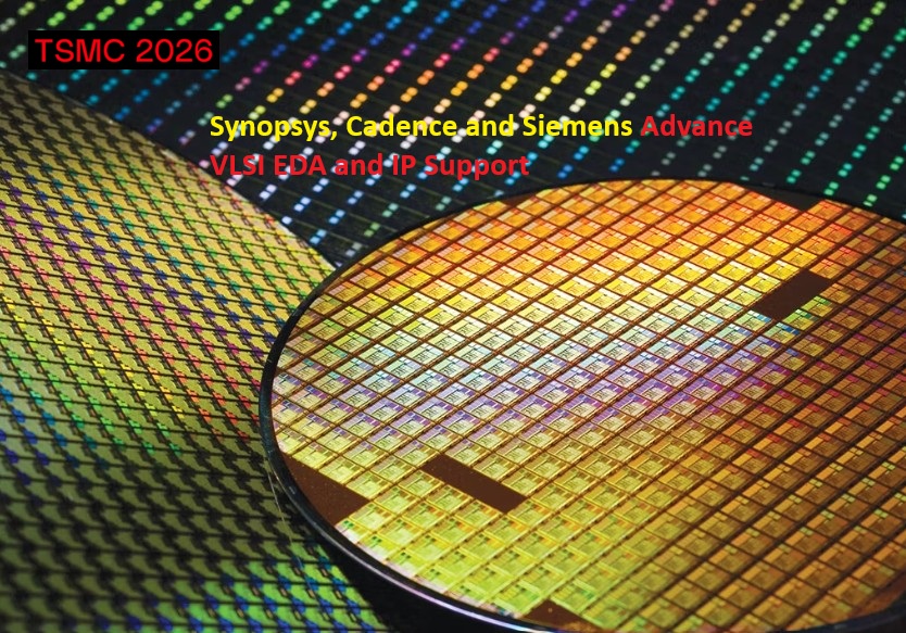
Synopsys, Cadence and Siemens Advance VLSI EDA and IP Support for Semiconductor Foundry Leader TSMC' 2nm, 3nm and A14 Nodes
Synopsys, Cadence, and Siemens announced updates to their collaborations with TSMC in sync with TSMC 2026 TECHNOLOGY SYMPOSIUM event conducted on 22nd Apr 2025 in Santa Clara CA US, covering silicon-proven IP, AI-powered VLSI EDA flows, and system-level enablement for TSMC's 3nm and 2nm adv
7 min read
TSMC Debuts A13 Process Technology at 2026 North America Technology Symposium
TSMC debuted its A13 process at the 2026 North America Technology Symposium in Santa Clara, California. The A13 process is a direct shrink of the A14 node announced in 2025. It provides 6% area savings from A14, with design rules fully backward compatible with A14. The technology uses nanosheet t
4 min read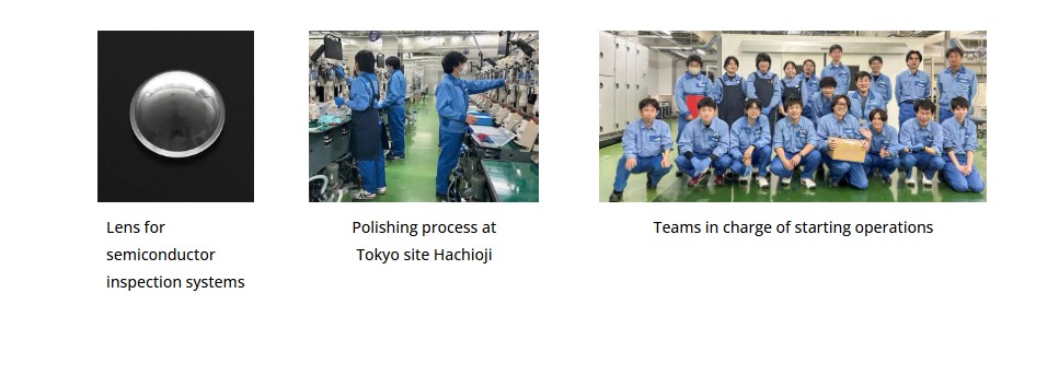
Konica Minolta Launches Lens Polishing Operations at Hachioji Tokyo Site for Semiconductor Inspection Equipment Optical Components
Konica Minolta, Inc. has established a new lens polishing process for optical components used in semiconductor inspection equipment at its Tokyo site in Hachioji and started operations at the end of March 2026. The move forms part of the company’s initiative to expand production capacity in
3 min read
Advantest Joins Applied Materials EPIC Platform as First ATE Company While Opening Silicon Valley Innovation Centers for AI HPC Semiconductor Test Solutions
Advantest announced the opening of two Advantest Innovation Centers—one located on the company's campus in San Jose, Calif., and another currently under construction in nearby Sunnyvale, Calif. The Advantest Innovation Center is a first-of-its-kind space offering state-of-the-art laboratori
6 min read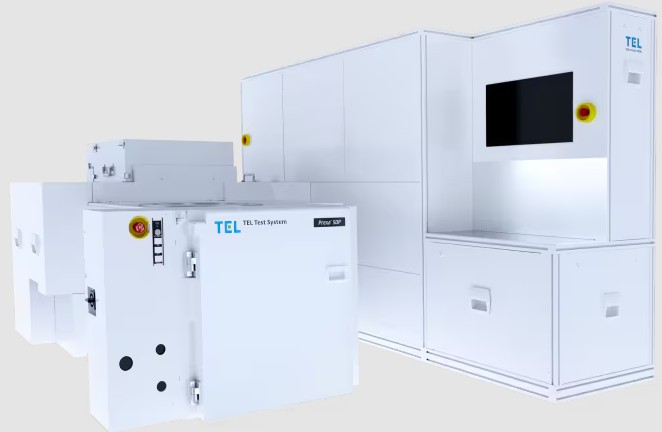
Tokyo Electron Launches Prexa SDP Device Prober for Singulated Device Testing in HPC and AI Semiconductor Applications
Tokyo Electron announced the launch of Prexa SDP, a device prober that meets the need for testing singulated devices. Demand for computing capability is surging. Advanced semiconductors used in high-performance computing and AI applications increasingly require the latest 2.5D/3D packaging techno
3 min read
Our Editors dive into topical news, new products, and discuss the shifting architecture of the global semiconductor industry.
▶ Podcast