Applied Materials announced a new innovation partnership with TSMC to develop materials, equipment, and process technologies for scaling next-generation semiconductor devices. The companies will work together at Applied’s EPIC Center in Silicon Valley.
The partnership builds on more than 30 years of collaboration. It aims to strengthen the innovation pipeline and accelerate the transition of breakthrough technologies from research to high-volume manufacturing. Focus areas include energy-efficient performance for AI applications from data centers to the edge.
“Applied and TSMC share a long history of deep collaboration built on trust and a shared commitment to advancing innovation at the leading edge of semiconductor technology,” said Gary Dickerson, President and CEO of Applied Materials. “By bringing our teams together at the EPIC Center, we are strengthening that partnership and accelerating the development of technologies to address the unprecedented complexity driving the chipmaking roadmap.”
Dr. Y.J. Mii, Executive Vice President and Co-Chief Operating Officer at TSMC, stated: “As semiconductor device architectures evolve with each new generation, the demands on materials engineering and process integration continue to increase. Meeting the challenges of AI at a global scale requires industry-wide collaboration. Applied Materials’ EPIC Center provides an ideal environment to accelerate equipment and process readiness for next-generation technologies.”

The collaboration at the EPIC Center targets materials engineering innovations for advanced logic scaling. Specific areas include:
- Process technologies enabling continuous power, performance, and area improvements across leading-edge logic nodes to address demands of AI and high-performance computing.
- New materials and next-generation manufacturing equipment for precise formation of complex 3D transistor and interconnect structures.
- Advanced process integration approaches to improve yield, variability control, and reliability in vertically stacked and highly scaled architectures.
Dr. Prabu Raja, President of the Semiconductor Products Group at Applied Materials, noted: “Advancing leading foundry technologies calls for a new model for collaboration and innovation. As a founding partner of the EPIC Center, TSMC gains earlier access to Applied’s innovation teams and next-generation equipment, helping accelerate the path from technology development to high-volume manufacturing.”
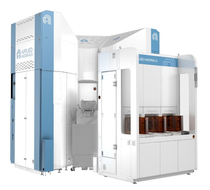
Applied’s EPIC (Equipment and Process Innovation and Commercialization) Center represents a $5 billion investment, the largest-ever U.S. investment in advanced semiconductor equipment R&D. The facility in Silicon Valley is designed to reduce the time required to commercialize breakthrough technologies from early-stage research to full-scale manufacturing. It is scheduled to become operationally ready in 2026 and will provide chipmakers with earlier access to Applied’s R&D portfolio, faster cycles of learning, and accelerated technology transfer in a secure collaborative environment. The center will also give Applied greater multi-node visibility to guide R&D investments.
In a related announcement, Applied Materials named Arizona State University (ASU), Rensselaer Polytechnic Institute (RPI), and Stanford University as inaugural research partners at the EPIC Center. These partnerships aim to accelerate the U.S. lab-to-fab innovation pipeline by combining academic research with commercial equipment and process expertise.

The university teams will work with Applied’s scientists and engineers on advanced materials, novel process and device technologies, and chip architecture developments. The EPIC Center offers an industry-scale R&D environment with access to cutting-edge chipmaking equipment for rapid co-innovation and faster commercialization.
Gary Dickerson said: “The EPIC Center is designed to bring together the best minds from industry and academia in a high-velocity, manufacturing-relevant environment to dramatically accelerate the development and commercialization of next-generation semiconductor technologies that are foundational to AI computing. Welcoming ASU, RPI and Stanford as research partners at EPIC strengthens the U.S. lab-to-fab innovation pipeline and creates a powerful platform for developing future semiconductor talent.”
Dr. Prabu Raja added that the partnerships build on Applied’s history of university collaborations and will advance discovery and commercialization through shared industry-academia efforts.
University leaders highlighted the benefits. Arizona State University President Michael Crow emphasized the alignment with industry needs and connection to ASU’s existing Materials-to-Fab Center with Applied. RPI President Martin Schmidt noted opportunities for faster lab-to-fab breakthroughs in materials, devices, and 3D integration, along with hands-on experience for students. Stanford’s H.S. Philip Wong pointed to the need for faster innovation cycles driven by AI growth and direct engagement with industry tools.
The EPIC Center enables university researchers to test materials integration in a manufacturing-relevant setting, supporting quicker validation and transition to deployment while contributing to workforce development in semiconductors.