Semiconductor and Component Equipment

Applied Materials, Intel, Besi and KIOXIA partner at Silicon Valley EPIC Center on AI chip technologies
Applied Materials announced it is working with Intel Corporation to develop next-generation transistors, interconnects, and advanced packaging technologies. The effort will use capabilities from Applied’s EPIC Center in Silicon Valley and Intel’s R&D campus in Hillsboro, Oregon. T
10 min read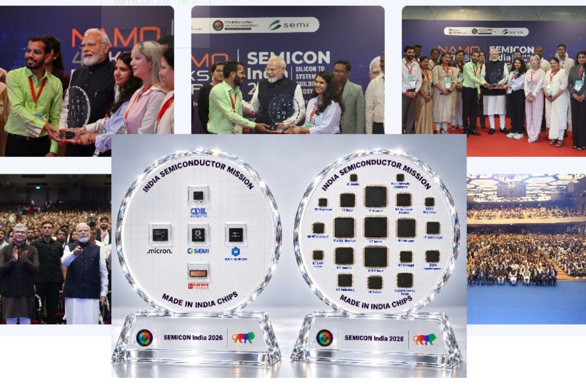
Who Showed Up: The Global Semiconductor Names Anchoring Semicon India 2026
More than 600 exhibitors and around 300 international companies filled Yashobhoomi over three days. A smaller group of names, however, set the tone for the entire event through the scale of what they announced, not just the size of their booths. Tata Electronics:&nbs
6 min read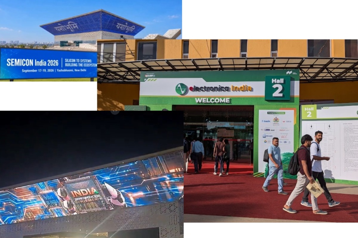
Four Years, A Different Country: How Fast India's Electronics and Semiconductor Landscape Has Actually Changed
Set the numbers from electronica India and productronica India 2026 alongside those from Semicon India 2026, and a single story emerges: in roughly four years, India's electronics and semiconductor design and manufacturing scenario has moved from policy announcements to commercial production line
7 min read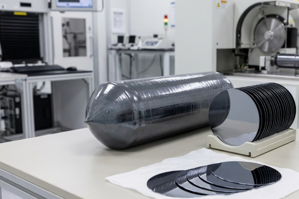
Crystal Clear: Why India's Semiconductor Ambitions Now Hinge on Silicon Crystal Growth
SEMICON India 2026 closed this past weekend at Delhi's Yashobhoomi Convention Centre, capping three days built around the theme "Silicon to Systems: Building the Ecosystem." The event drew more than 600 companies and delegations from 52 countries. But beneath the headline investment announcements
10 min read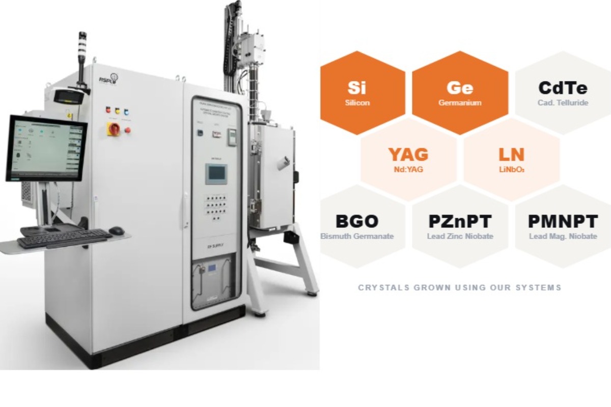
Silicon Sovereignty: How One Indian Company Is Racing to Localize Semiconductor Crystal Growth Technology
A decade-old company is trying to close one of the most overlooked gaps in India's semiconductor and solar ambitions, the crystal growth technology that turns raw silicon into usable wafers. India's semiconductor strategy has largely centered on fabrication plants and chip
13 min read
Qatar Airways Cargo Adds VRR Containers for Semiconductor Equipment
Qatar Airways Cargo has added Van Riemsdijk Rotterdam’s (VRR) specialised RGX and RZY containers to its portfolio to support the transportation of advanced capital equipment within the semiconductor industry. The climate-controlled containers form part of the carrier’s TechLift transp
2 min read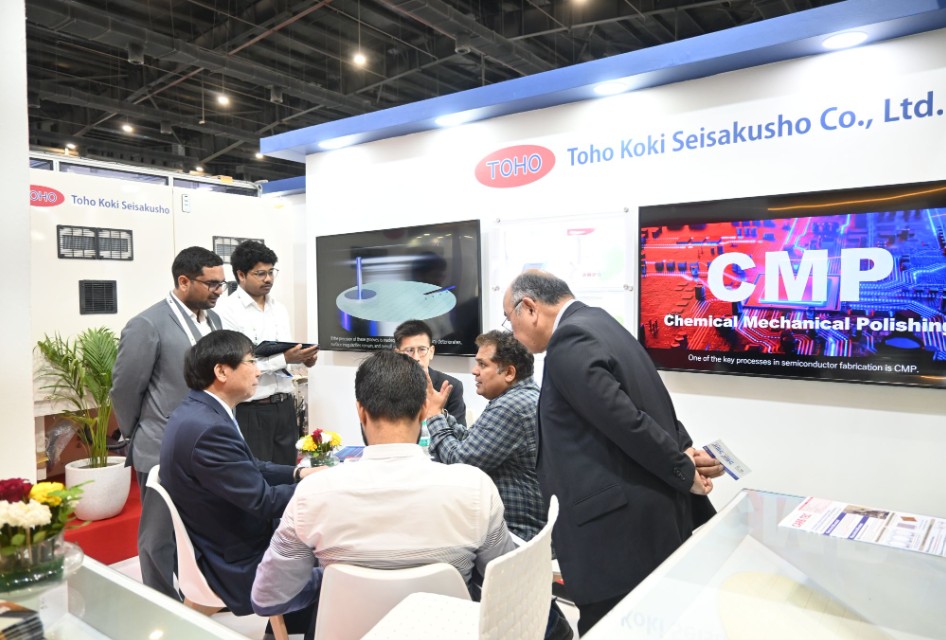
Inside Toho Koki's Push Into India's Semiconductor Manufacturing Ecosystem
Japanese semiconductor equipment maker Toho Koki Seisakusho Co., Ltd. is steadily building a foothold in India, courting academic institutions, state-run innovation hubs, and private companies as it positions the country as a key partner for future semiconductor manufacturing.
6 min read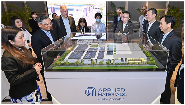
How Applied Materials Built a Two-Headed Engine in Singapore and India
The first installment of our series profiles Applied Materials—a legacy giant making massive waves in the Indian semiconductor ecosystem. As proud participants in “CoseIn 2026” (organized by IISc Bangalore, with “EE Herald” serving as Media Partner), we wan
13 min read
ZEISS Opens New Production and Office Building in Oberkochen for Semiconductor Operations
ZEISS Semiconductor Division has inaugurated a new production and office building at its headquarters in Oberkochen, Germany. The facility spans more than 23,000 square meters, equivalent to just over three football fields, and is designed for future growth. ZEISS supplies critical optical
2 min read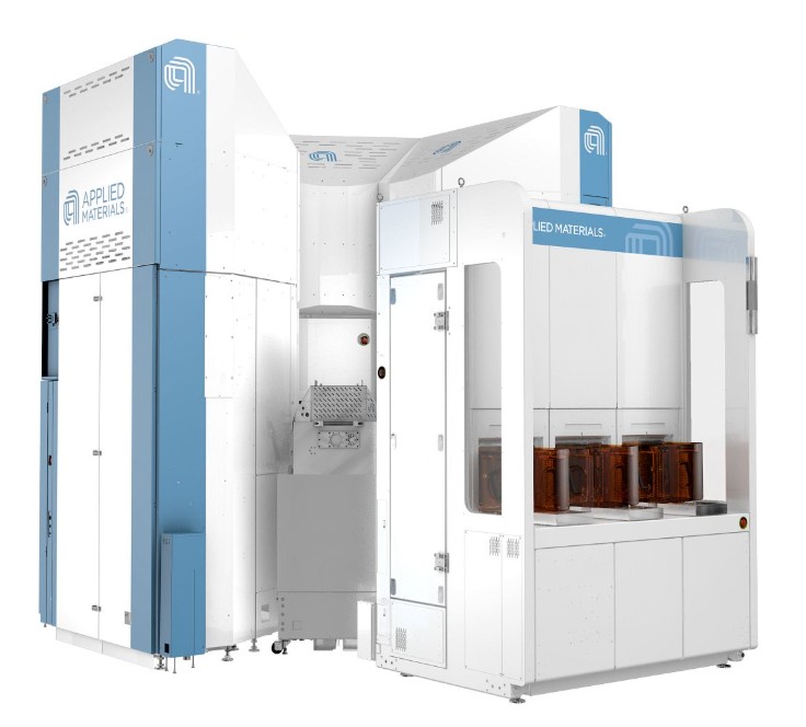
Applied Materials Introduces New Systems for DRAM and Advanced Packaging Supporting AI Chip 3D Architectures
Applied Materials introduced a suite of new chipmaking systems for building advanced 3D chip architectures used in next-generation AI. The announcement addresses constraints in AI compute where model scale and data movement demands outpace gains in bandwidth, capacity and energy efficiency
6 min read
SEMICON West 2026 Returns to San Francisco October 13-15
SEMI announced that SEMICON West 2026 will take place October 13-15 at the Moscone Center in San Francisco. The event returns to the Bay Area after last year’s event in Phoenix. Registration is now open, with early-bird rates available until June 26. The semiconductor industry is expected t
3 min read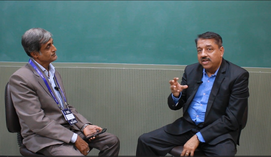
Applied Materials Executive Says India Has Opportunity to Move from Participant to Shaper of Global Semiconductor Industry
Dr Suraj Rengarajan, Managing Director and Principal Technologist at Applied Materials India, opened his remarks at COSEIn 2026 with a personal note: he moved to India in 2007, he said, because he was told a fab was coming. "And so it's finally here." Re
5 min read
Our Editors dive into topical news, new products, and discuss the shifting architecture of the global semiconductor industry.
▶ Podcast