Applied Materials Introduces New Systems for DRAM and Advanced Packaging Supporting AI Chip 3D Architectures
Applied Materials introduced a suite of new chipmaking systems for building advanced 3D chip architectures used in next-generation AI.
The announcement addresses constraints in AI compute where model scale and data movement demands outpace gains in bandwidth, capacity and energy efficiency. This situation has accelerated adoption of advanced packaging architectures including high bandwidth memory and 3D stacking.
Enhanced epitaxy system for DRAM
Applied Materials introduced an enhanced Centura Prime Epi system optimized for DRAM fabs. The system selectively grows doped silicon germanium and silicon phosphorous in source/drain regions of peripheral transistors. It combines advanced strain engineering with precise doping control. The result is higher drive current and transistor efficiency, enabling faster and more power-efficient DRAM operation required for high bandwidth memory and next-generation DDR.
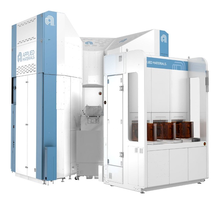
The new system has a 20 percent smaller footprint than prior versions.
Dr. Prabu Raja, President of the Semiconductor Products Group at Applied Materials, stated: “The transistor and materials technologies that drove performance gains in leading-edge logic are now becoming e...