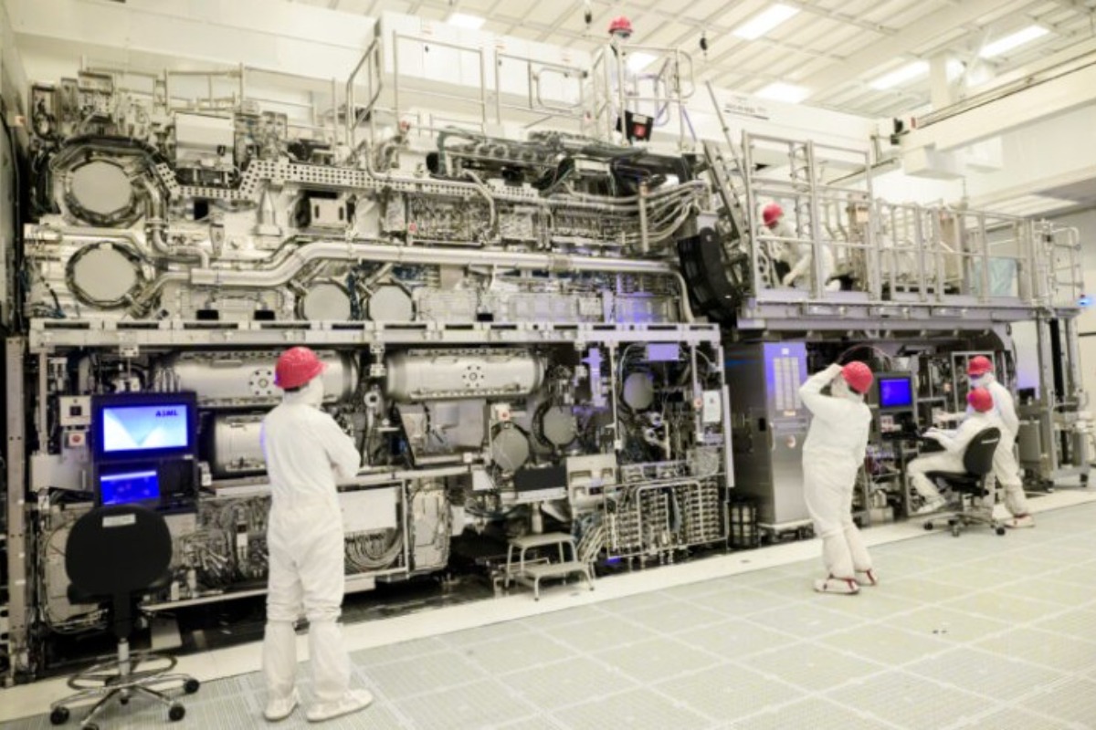
Advantest announced the opening of two Advantest Innovation Centers—one located on the company's campus in San Jose, Calif., and another currently under construction in nearby Sunnyvale, Calif. The Advantest Innovation Center is a first-of-its-kind space offering state-of-the-art laboratories and advanced test equipment. The facilities are designed to enable deep collaboration with partners across the semiconductor value chain, accelerating the development of innovative test solutions for next-generation semiconductor technologies.
Separately, Advantest announced that it will join Applied Materials' new EPIC (Equipment and Process Innovation and Commercialization) platform in Sunnyvale, Calif. As the first automated test equipment (ATE) company to join the platform, Advantest will partner with Applied to strengthen the links between front-end manufacturing technologies and back-end testing of chips and packages.
This partnership aligns with Advantest's recently launched Innovation Center, which fosters cross-functional collaboration to accelerate the development of advanced test solutions for next-generation semiconductor technologies. Advantest's Innovation Center provides state-of-the-art labs and research facilities equipped with the latest technology to support a wide range of R&D programs and will seamlessly connect with Applied's EPIC Center, opening later this year.

With the rising complexity of artificial intelligence (AI), high-performance computing (HPC) and edge devices, cross-ecosystem collaboration has become increasingly important to meet future industry needs. Leveraging expertise across the supply chain is essential to develop innovative test solutions that can overcome the challenges of advanced packaging, increasing data capacity and evolving quality and reliability standards.
The Advantest Innovation Centers provide a unique environment to support this collaboration, featuring state-of-the-art equipment, clean rooms and the latest test technologies and test insertions for advanced packaging and complex device architectures. Strategically located in Silicon Valley, these facilities offer a central hub for hands-on innovation, enabling the company's partners to work side by side with Advantest's team of experts to develop innovative solutions that optimize reliability and improve productivity. Partnering early in the development process allows participants to build informed, long-term roadmaps and align R&D efforts to address industry challenges from the outset. Through these collaborations, the Advantest Innovation Centers will help deliver cutting-edge test solutions that innovate workflows to support the needs of customers in high-performance computing, edge AI, and other emerging markets worldwide.
As advanced packaging drives increasing complexity in the architecture of high-performance computing (HPC) semiconductors, close collaboration between Advantest and leading manufacturing companies across the supply chain has become critical in overcoming complex challenges and delivering innovative test solutions to customers. This unique partnership allows Advantest and Applied Materials to align their expertise in anticipating customer needs and developing fully integrated solutions that optimize performance, enhance efficiency, increase yield and reduce time-to-market when testing next-generation semiconductors.
"These Innovation Centers represent a major milestone in how we work with our partners to drive innovation," said Kotaro Hasegawa, senior vice president of the New Research Platform Initiative, Advantest. "Cross-industry collaboration is a critical step in accelerating innovation for high-performance computing and edge AI applications, as advanced packaging and increasingly complex device architectures demand new approaches to test."

"We are excited to have Advantest join our EPIC platform as an innovation partner, and we look forward to our teams collaborating to accelerate end-to-end semiconductor technology development for the AI era," said Gary Dickerson, president and chief executive officer, Applied Materials. "Working alongside Advantest, we aim to co-develop solutions that optimize semiconductor production flows for faster prototyping and improve the energy-efficient performance of next-generation computing systems."
"As devices become increasingly complex, we provide opportunities to collaborate with partners from the very early stages of the semiconductor manufacturing process," said Doug Lefever, representative director and group CEO of Advantest Corporation. "We believe this partnership will facilitate joint development work that yields scalable and cost-effective testing methodologies for customers' next-generation technologies. This enables us to build optimal solutions early on to meet industry needs, establishing a framework to respond swiftly and efficiently to future demand."
The Advantest Innovation Center located in San Jose is open, while the Sunnyvale location is planned to open later this summer. Partnerships have already been initiated with leading manufacturers and suppliers. For more information, please visit the company's website.