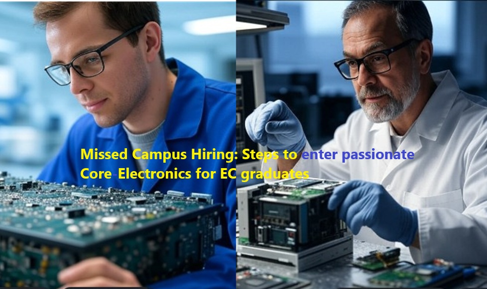
Approximately 80% of electronics and communication engineering graduates end up in software or IT jobs. However, intense competition from computer science, information science, AI, and machine learning graduates makes securing these roles challenging. Even if you land a software job, it may not a
Read more: https://www.eeherald.com/section/news/p20250603nwcareercore.html
Essential software programming skills for VLSI engineers
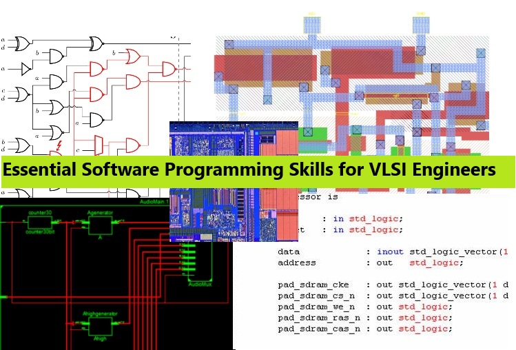
VLS (Very Large-Scale Integration) engineer requires more than just theoretical knowledge of electronics—it demands proficiency in specialized software tools that bring chip designs to life. These Computer Aided Design (CAD) tools, known as Electronic Design Automation (EDA) software, are
Read more: https://www.eeherald.com/section/new-products/p20250604nwbellivlsi3.html
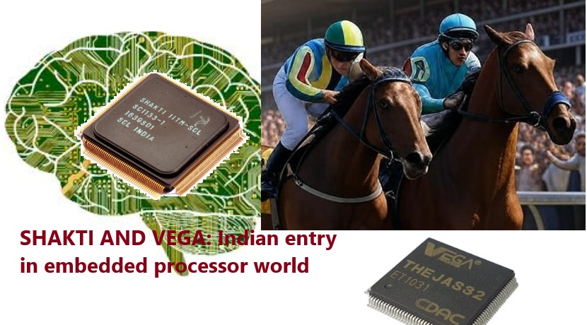
Embedded systems need a powerful processor/microcontroller and software IDE platform and support packages at core. With these basics, embedded systems also require few CAD/EDA tools to design the board. Lot of other semiconductor devices such as analog, power, and wireless interface ICs too
Read more: https://www.eeherald.com/section/news/p20250603nwvegashati01.html
Top destinations for higher education in semiconductor and VLSI outside US
With recent U.S. restrictions on foreign students, particularly at prestigious institutions like Harvard, concerns are growing about further limitations on international students pursuing higher education in the U.S. Many Indian electronics engineering graduates traditionally seek postgraduate st
Read more: https://www.eeherald.com/section/news/p20250602nwraiwan.html
Analysis of the cleanroom market in India for semiconductor manufacturing
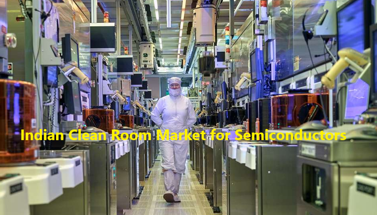
India’s accelerated push to develop a robust semiconductor manufacturing ecosystem is driving significant growth in the cleanroom market for semiconductor fabrication and research laboratories. This growth aligns closely with the expansion of the semiconductor industry. Additionally, precis
Read more: https://www.eeherald.com/section/news/p20250601nwcleanmarket.html
Cleanroom in semiconductor manufacturing: Basic essential of a chip fab
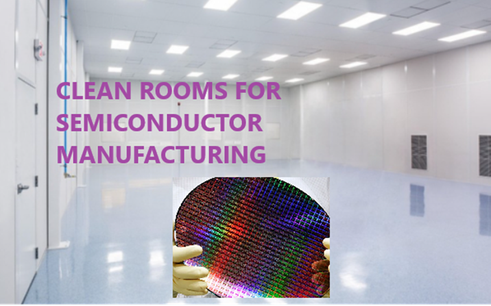
When manufacturing semiconductor devices with features as small as 2 nanometers, even a speck of nearly invisible dust, approximately 1 micron in size, adhering to the wafer can render the device defective, leading to significant losses due to rejected wafers. To ensure high-quality production,
Read more: https://www.eeherald.com/section/new-products/p20250601nwcleanroombasic2.html
PTW Group appoints Venkatesh Pandurengan as General Manager of Its new Indian subsidiary

PTW Group, a global leader in semiconductor engineering solutions, specializes in legacy equipment repair, refurbishment, trading, proprietary equipment production, wafer production line setup, parts supply, equipment upgrades, maintenance, training, and repair services for semiconductor Fabs, OS
Read more: https://www.eeherald.com/section/news/p20250602nwptwvenkatesh.html
Essential skills for a successful VLSI chip design engineering career
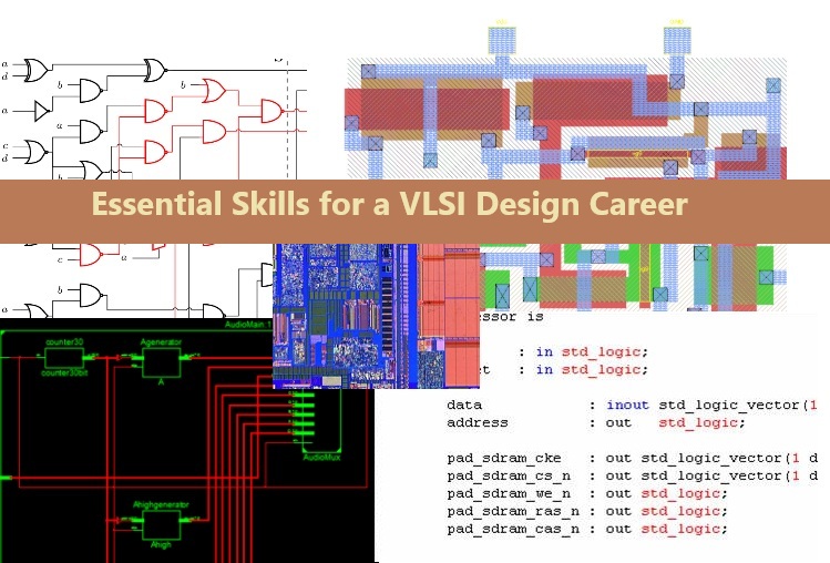
Becoming a VLSI (Very Large Scale Integration) semiconductor chip design engineer is both a well-paid and satisfying career path that combines deep technical knowledge with innovative problem-solving. If you're aspiring to excel in this field, here's a rundown of the essential skills you'll
Read more: https://www.eeherald.com/section/news/p20250604nwbellivlsi2.html
A journey to becoming a VLSI semiconductor chip design engineer
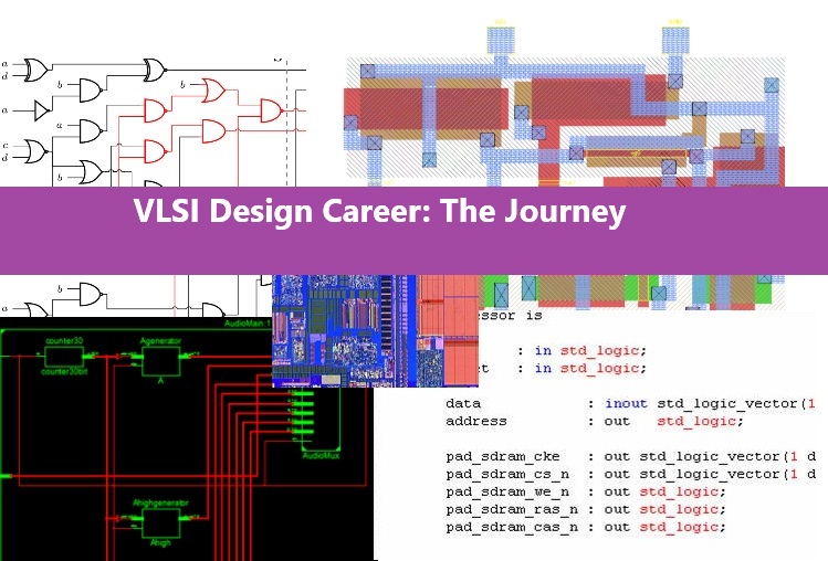
Imagine holding a smartphone, its sleek design hiding a marvel of engineering: a chip smaller than a coin, yet packed with billions of transistors working in harmony to power your apps, calls, and AI assistants. This is the magic of Very Large-Scale Integration (VLSI) design, the art and science
Read more: https://www.eeherald.com/section/news/p20250604nwbellivlsi1.html
TIEA Connectors Private Limited, a B2B electronic system design and manufacturing (ESDM) startup, has raised INR 22 crore in a funding round led by Jamwant Ventures and Valour Capital, with participation from 8X Ventures and IvyCap. The funds will be utilized to expand manufacturing capacity, enh
Read more: https://www.eeherald.com/section/news/p20250603ntiea.html

IPC announced it is accepting abstracts for technical papers, posters, and professional development courses for IPC APEX EXPO 2026. The event, featuring the renamed Advanced Electronic Packaging Conference 2026: Component- to System-Level Integration, will occur March 17-19, 2026, with profession
Read more: https://www.eeherald.com/section/news/p20250604nwipc.html
MaxLinear and Comtrend launch powerline data modules for EV charging stations

MaxLinear and Comtrend announced the availability of ITU-T standards-based powerline data modules for electric vehicle (EV) charging station (EVSE) backend communication, including data centers and smart parking extensions. The modules, utilizing MaxLinear’s G.hn technology, enable Comtrend
Read more: https://www.eeherald.com/section/news/p20250604nwmaxlinear.html
Cadence and Arm collaborate to advance automotive chiplet ecosystem with Arm Zena compute subsystems

Cadence has announced IP, design solutions, and expert design services for software and Systems-on-Chip (SoCs) based on Arm Zena Compute Subsystems (CSS), Arm’s first-generation CSS for automotive applications, as part of a 2024 collaboration to accelerate the automotive chiplet ecosystem.
Read more: https://www.eeherald.com/section/news/p20250604nwcaden.html
GlobalFoundries to invest $16 billion in U.S. semiconductor manufacturing expansion

GlobalFoundries announced a $16 billion investment to expand its semiconductor manufacturing and advanced packaging capabilities in New York and Vermont. The initiative, supported by the Trump Administration and technology companies including Apple, SpaceX, AMD, Qualcomm Technologies, Inc., NXP,
Read more: https://www.eeherald.com/section/news/p20250604nwgf.html
Strategic materials conference 2025 to address semiconductor manufacturing innovations

The Strategic Materials Conference (SMC) 2025, scheduled for June 23-25 at Hayes Mansion in San Jose, California, will focus on materials innovation for semiconductor manufacturing. The event will bring together executives and technology leaders to discuss trends and advancements in the field. Re
Read more: https://www.eeherald.com/section/news/p20250602nwsemi.html
Global Semiconductor Forum addressed supply chain challenges in Taipei
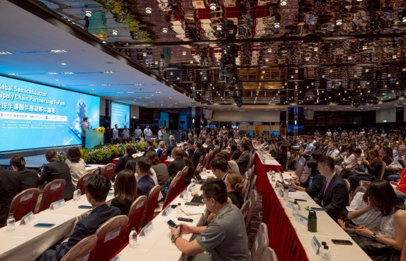
On May 23, 2025, the Global Semiconductor Supply Chain Partnership Forum took place in Taipei, Taiwan, focusing on collaboration among democratic nations to strengthen semiconductor supply chains. The event, organized by Taiwan’s Industrial Technology Research Institute (ITRI), drew over 70
Read more: https://www.eeherald.com/section/news/p20250602nwgssttaipei.html