Nano Semiconductor Fab

SCREEN and IBM Collaborate on High NA EUV Lithography Cleaning Process Development
SCREEN Semiconductor Solutions Co., Ltd. and IBM have entered into an agreement to develop cleaning processes for next-generation EUV lithography, focusing on High NA (High Numerical Aperture) EUV technology. This collaboration extends a partnership spanning over a decade, previously centered on
2 min read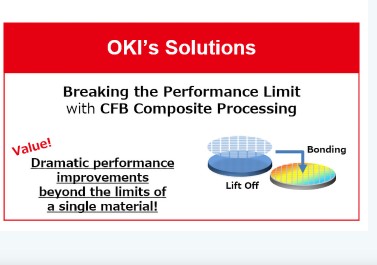
OKI Advances Photonics Integration with Tiling CFB Technology for 300 mm Silicon Wafers
OKI has developed Tiling Crystal Film Bonding (CFB) technology, enabling the heterogeneous integration of small-diameter optical semiconductor wafers, such as 50 mm to 100 mm indium phosphide (InP) wafers, onto 300 mm silicon wafers. This addresses previous limitations due to wafer size dis
4 min read
Smartkem and Manz Asia Announce Preliminary Joint Development Agreement for AI Chip Packaging Dielectric Ink Solutions
Smartkem, a company focused on transistor technology, has entered into a preliminary, non-binding Joint Development Agreement (JDA) with Manz Asia, a developer of advanced packaging equipment for the semiconductor industry. The agreement, when finalized, will center on co-developing dielectric in
2 min read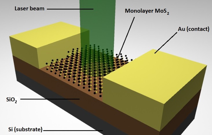
University of Michigan study reveals safer method for synthesizing 2D Molybdenum Disulfide
A research team at the University of Michigan has published a study in the Chemistry of Materials Journal demonstrating a new method for synthesizing high-quality two-dimensional (2D) molybdenum disulfide (MoS2) using Veeco Instruments Inc.’s Fiji G2 plasma-enhanced atomic layer deposition
2 min read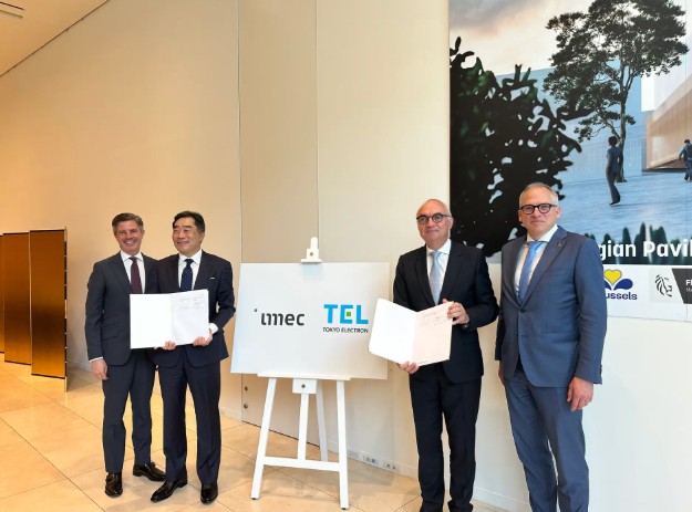
Imec and Tokyo Electron extend partnership for beyond-2nm semiconductor development
Imec, a research hub in nanoelectronics and digital technologies, has extended its strategic partnership with Tokyo Electron (TEL), a Japanese supplier of semiconductor production equipment, for an additional five years. The agreement aims to advance joint research and development in next-generat
3 min read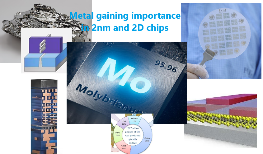
Molybdenum role in 2D and 2nm GAA semiconductor chip fabrication rising the demand for this metal
Copper dominated as metal interconnect in chips for decades, however now at 2nm with vertically forming gate all around (GAA) transistors and future Complementary-Field Effect Transistor (CFET), Copper is creating problems such as high diffusivity, voids in filling, and Edge-Placement Errors (EPE
8 min read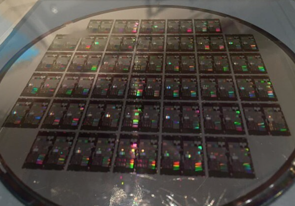
IEEE study: Silicon photonic AI accelerators utilizing ONNs for scalable and sustainable AI hardware
A study published in the IEEE Journal of Selected Topics in Quantum Electronics describes a new AI acceleration platform using photonic integrated circuits (PICs). Led by Dr. Bassem Tossoun of Hewlett Packard Labs, the research focuses on improving scalability and energy efficiency for AI workloa
4 min read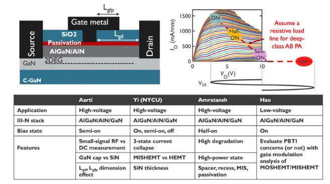
Enhancing reliability of GaN MISHEMTs in RF power amplifiers for next-gen communication systems
At the IEEE International Reliability Physics Symposium 2025, imec announced a significant breakthrough in the stability of GaN MISHEMTs (Metal-Insulator-Semiconductor High Electron Mobility Transistors) for RF power amplifiers. Despite challenges with positive bias (on-state) instability, imec's
5 min read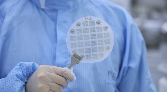
Chinese researchers develops world’s first 1nm thin RISC-V chip using 2D materials
Chinese scientists have created the world’s most advanced two-dimensional (2D) semiconductor microprocessor, named Wuji. This 32-bit RISC-V chip, less than 1 nanometre thick, integrates 5,900 transistors. The research, led by Professors Bao Wenzhong and Zhou Peng from Fudan University&rsquo
4 min read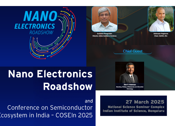
Nano Electronics Roadshow: Conference on semiconductor eco systems in Bengaluru, India on 27th March
The Nanotechnology Initiatives Division of MeitY in partnership with premium institute IISc Bengaluru, IIT Bombay, IIT Madras, IIT Delhi, IIT Kharagpur, and IIT Guwahati is organizing the Nano Electronics Roadshow and Conference on Semiconductor Ecosystem in India. The event is scheduled fo
3 min read
Our Editors dive into topical news, new products, and discuss the shifting architecture of the global semiconductor industry.
▶ Podcast