From Design to Fab: GeniSys Tools That Make Your Semiconductor Designs Manufacturing-Ready, Listen to Genisys' Executives
Transcript
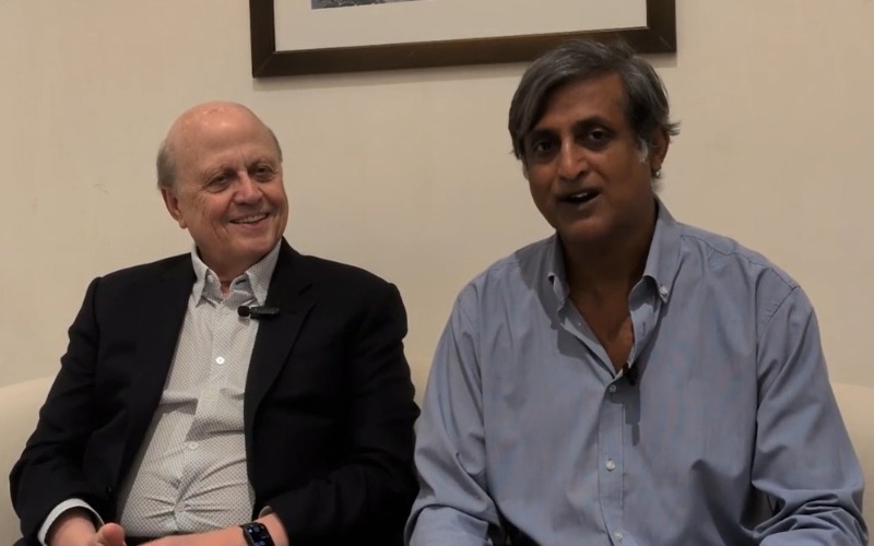
Hi, welcome to our interactive talk with two executives from genisys who are very much into (0:22) advanced semiconductor manufacturing, more than hardware, they are into software.
Host: (0:26) Me, editor of EEHerald, interacting with Kaustubh and Dimitri.
Kaustubh, welcome to (0:33) the talk. Thank you, Dimitri. Welcome to the talk.
I have few questions on your products and services (0:39) very relevant to Indian semiconductor manufacturing and what exactly happening now. (0:46) Basically, can you first initially tell about what is Genesis current strategy and long-term (0:53) vision for the Indian semiconductor ecosystem, especially with the growing number of design (0:58) centers and upcoming manufacturing facilities in India?
Kaustubh: So yeah, there's a lot happening in the (1:07) Indian semiconductor space right now. A lot of good things.
About this edition
How GeniSys Solutions Help Indian Semiconductor Companies - Designers produce files such as GDS files for manufacturing. - These files are used in electron beam lithography, laser lithography tools, or sent to large fab houses. - During lithography, deleterious effects occur that can alter the intended structures (e.g., a designed 100 nm waveguide or channel may result in 80 nm or 120 nm). - GeniSys software corrects for these effects, ensuring the manufactured result matches the original design exactly. - This improves manufacturability, makes designs production-ready, and ensures machine-readable outputs. - Solutions also support simulation (e.g., optical lithography), process optimization and stability, and metrology/inspection after production.
SiliconBridge is a product of EE Herald. We independently explore the nexus between industry, academia and past, prevailing and potential future geopolitical architectures
More episodes
The Basketball NYC Knicks win, SpaceX IPO, Elon Musk becomes the first ever Trillionaire, Employing AI to prevent and contain fires in CA, and CoseIn (Bengaluru) is on with the heavy lifters Lam Research, Horiba, Tokyo Electron, MsDermid Alpha, ISRO….
The Basketball NYC Knicks win, SpaceX IPO, Elon Musk becomes the first ever Trillionaire, Employing AI to prev

Newscast for the week of June 15 2026
We are covering the following: India’s Growing Semiconductor Ecosystem Major Manufacturing & Fab Construction

Silicon Bridge - DC to Delhi: Were talking about the AI Bubble, TSMC in Arizona, and the CoseIn event in Bangalore.
The AI Bubble—Bursting or Just Evolving? TSMC has started 3nm chips production in the US. Bangalore Event (C
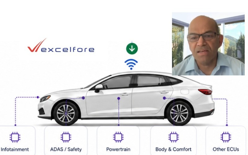
Software-Defined Vehicles: Execution Challenges and the Case for Standardization — Insights from Excelfore CEO Shrinath Acharya
In this exclusive interview, Srinivasa Reddy N, Editor of EEHerald, speaks with Shrinath Acharya, CEO & Co-fou
Not so easy -- issues between India and the US. And other top stories.
Welcome to the Silicon Bridge: DC to Delhi brought to you by the Electronics Engineering Herald, India's leadi
Semiconductor Legend Wally Rhines on TSMC Dominance, AI Boom & EDA Future
In this exclusive deep-dive interview, semiconductor industry icon Dr. Walden "Wally" Rhines—CEO of Silvaco Gr