In the presence of Ashwini Vaishnaw, Union Minister for Railways, Information & Broadcasting, and Electronics & IT, Qualcomm Technologies, Inc. announced the completion of the tape-out for its 2-nanometer semiconductor design. The design process involved significant contributions from the company's engineering centers in Bengaluru, Chennai, and Hyderabad.
This marks Qualcomm's largest engineering workforce outside the United States, with India serving as its primary engineering hub beyond domestic operations. The company has maintained continuous investment in India for more than two decades, building capabilities in wireless technologies, compute, artificial intelligence, and system-level engineering. Teams in India handle design implementation, validation, AI optimization, system integration, architecture contributions, and software platforms for global products used in billions of devices.

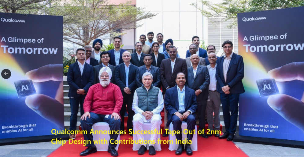
The milestone was presented at Qualcomm's Bengaluru facility during a visit by Ashwini Vaishnaw. Vaishnaw stated that India is increasingly central to the design of advanced semiconductor technologies for the future. He described the development as evidence of the maturity of India's design ecosystem and its alignment with the goal of establishing a globally competitive semiconductor industry.
Srini Maddali, Senior Vice President of Engineering at Qualcomm India, noted that the 2nm tape-out confirms the engineering depth in the country, with India teams delivering at global standards in collaboration with worldwide program and architecture groups.

Savi Soin, President of Qualcomm India, said India plays a key role in supporting the design, development, and delivery of next-generation technologies for connectivity, computation, and intelligent systems globally.
Amitesh Kumar Sinha, Additional Secretary in the Ministry of Electronics and IT and CEO of the India Semiconductor Mission, commented that the mission is advancing with momentum through a strengthening design ecosystem and industry participation. He emphasized that investments in advanced engineering and R&D are essential for long-term semiconductor capacity in India.
The announcement occurs as India pursues policies, incentives, and partnerships to establish itself as a global semiconductor hub. It follows MediaTek's earlier tape-out of a 2nm chip announced in 2025 for TSMC's process, with volume production targeted for late 2026, amid competition among major players including Apple, MediaTek, and Samsung for advancements on next-generation manufacturing nodes.