SK hynix Inc. presented its DRAM technology roadmap for the next 30 years at the IEEE VLSI Symposium held in Kyoto, Japan, from June 8-12, 2025. The company addressed challenges and proposed innovations to advance DRAM technology.
During a plenary session on June 10, Chief Technology Officer Cha Seon Yong discussed limitations in improving performance and capacity with current DRAM scaling technology. He announced that SK hynix plans to adopt the 4F² Vertical Gate (VG) platform and 3D DRAM technology for 10-nanometer or smaller processes. The 4F² VG platform aims to minimize cell area, enabling higher integration, faster speeds, and lower power consumption through a vertical gate structure. Unlike the current 6F² cells, the 4F² cell, combined with wafer bonding technology, places circuits below the cell area to enhance efficiency and electrical characteristics.
Cha also highlighted 3D DRAM as a key component of future DRAM development. Despite industry concerns about potential cost increases due to stacked layers, he stated that ongoing technological innovation could address these challenges. SK hynix aims to advance critical materials and components to support DRAM development over the next three decades.
Reflecting on past progress, Cha noted that DRAM technology was once expected to hit limitations at 20 nanometers around 2010, but innovations have extended its viability. He emphasized SK hynix’s commitment to guiding long-term innovation and collaborating with the industry to shape the future of DRAM.
On the final day of the symposium, Joodong Park, vice president of SK hynix’s Next Gen DRAM Task Force, will present research on the impact of VG and wafer bonding technology on DRAM’s electrical characteristics.
SK hynix outlines DRAM technology roadmap at IEEE VLSI symposium 2025
Listen to this story
ⓘ AI NARRATED0:00 / 0:00
More from Memory →

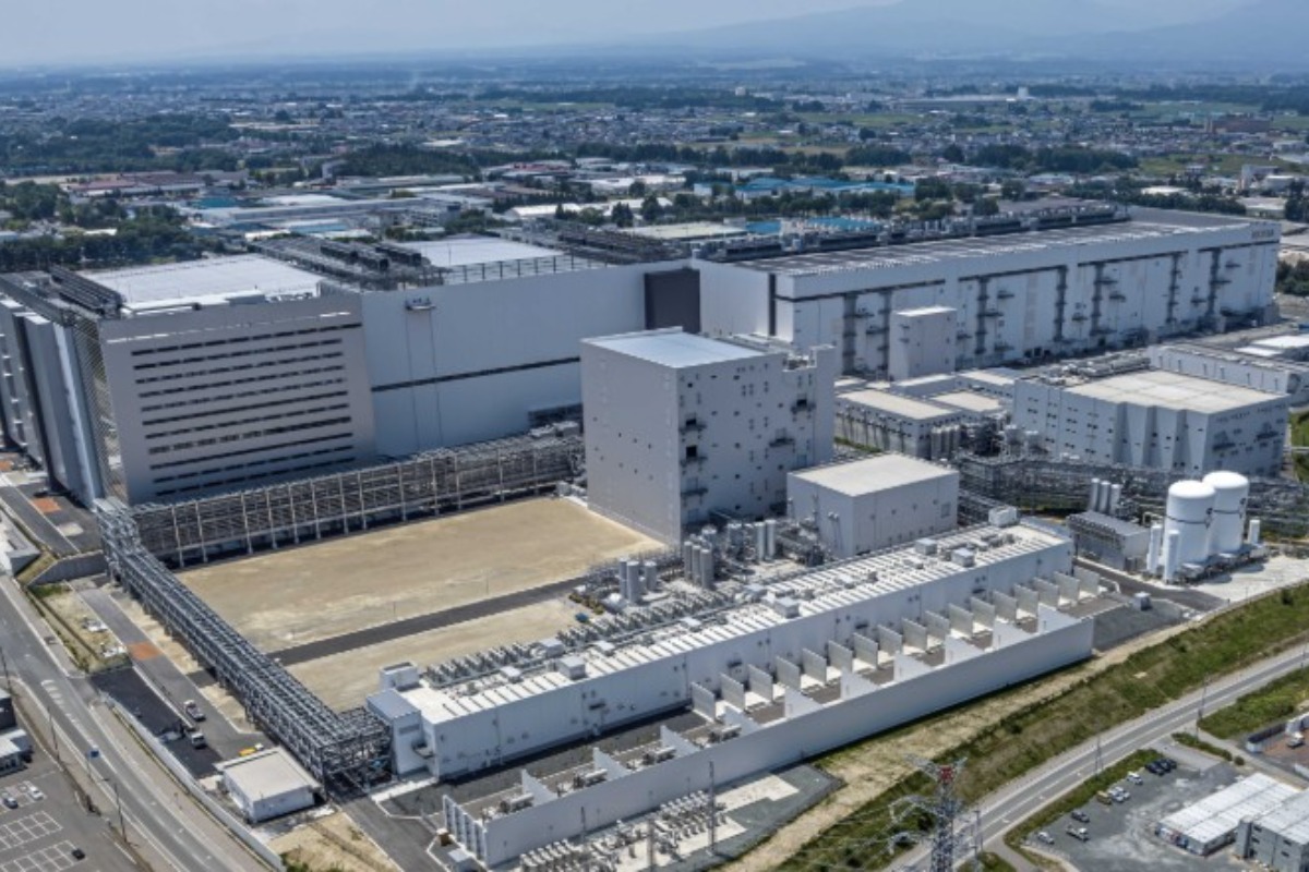
Micron Breaks Ground on $9.3 Billion HBM Expansion in Hiroshima Factory
Micron has started construction on a ¥1.5 trillion ($9.3 billion) expansion at its semiconductor factory in Higashihiroshima City, Hiroshima Prefecture,…
Kioxia and Sandisk Begin 10th-Generation 3D NAND Production at Kitakami Fab2 as Sandisk Samples BiCS10 1Tb TLC 3D NAND Flash Memory
Kioxia and Sandisk have begun production of their 10th-generation 3D flash memory…
GigaDevice Enters EEPROM Market with New GD24CL I²C Series
GigaDevice, a semiconductor company specializing in Flash memory, 32-bit microcontrollers (MCUs), sensors,…