Toshiba Electronic Devices & Storage Corporation announced on June 9, 2025, the development of two technologies for silicon carbide (SiC) power semiconductors aimed at reducing losses in high-efficiency power conversion applications, such as electric vehicles and renewable energy systems. The technologies address challenges in SiC trench MOSFETs and SiC Schottky barrier diodes (SBDs) related to on-resistance and reliability in high-temperature environments.

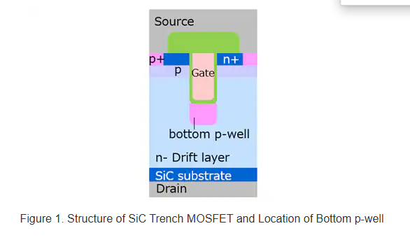
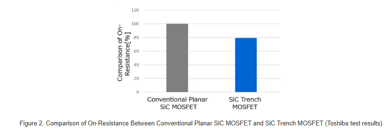
For SiC trench MOSFETs, Toshiba developed a method to improve unclamped inductive switching (UIS) ruggedness by forming a Bottom p-well protective layer in the trench structure and reducing the grounding resistance of the electric field protection structure. This approach clarified the relationship between UIS ruggedness and grounding resistance, which was previously uncertain. Prototyped SiC trench MOSFETs achieved a 20% reduction in on-resistance compared to conventional planar SiC MOSFETs.
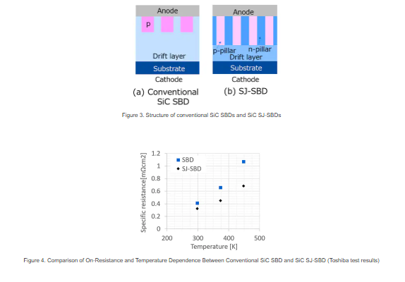
For SiC SBDs, Toshiba developed semi-super-junction Schottky barrier diodes (SJ-SBDs) with alternating p-type and n-type pillars in the drift layer to suppress on-resistance increases at high temperatures. The SJ structure creates a flat electric field distribution, reducing resistance. Testing showed that 650V SiC SJ-SBDs reduced on-resistance by 35% at 175°C compared to conventional SiC SBDs.

These technologies are expected to enhance the reliability and efficiency of power conversion devices. Toshiba presented the developments at the 37th International Symposium on Power Semiconductor Devices and ICs (ISPSD) 2025 in Kumamoto, Japan, held from June 1 to 5. The work was supported by a project subsidized by the New Energy and Industrial Technology Development Organization (NEDO). Toshiba plans to further refine these technologies for early practical application.