Keysight Technologies, introduced 3D Interconnect Designer, a new tool added to its Electronic Design Automation (EDA) portfolio. The solution targets the complexity involved in designing 3D interconnects for chiplet-based and 3DIC advanced packages in AI infrastructure and data center applications.
Chiplet architectures have increased the challenges in 3D interconnect designs for multi-die and stacked-die systems. Traditional workflows require significant manual effort to optimize elements such as vias, transmission lines, solder balls, and micro-bumps while maintaining signal and power integrity in dense configurations. This leads to additional design iterations, extended development cycles, delayed product launches, and higher costs.

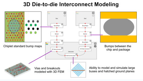
The 3D Interconnect Designer provides a dedicated workflow to design, optimize, and validate 3D interconnects. It manages complex geometries, including hatched or waffled ground planes, which address manufacturing constraints in silicon interposers and bridges for advanced packages.
Key features include:
Automation of workflows to reduce manual steps, limit errors, and improve first-pass success rates.
Validation against standards such as UCIe, BoW, and ex VTF early in the design process to lower the risk of late-stage redesigns.
Electromagnetic-based simulation for accurate electrical analysis of PCB and package-level 3D interconnects.
The tool integrates with other Keysight EDA software and is available as a standalone version. When used with Chiplet PHY Designer, it supports specific design and optimization of 3D interconnects for chiplets and 3DICs in multi-die systems.

Nilesh Kamdar, EDA Design and Verification General Manager at Keysight, stated that manual 3D interconnect design has become a bottleneck due to increasing complexity. The tool provides early visibility into signal and power integrity issues to support faster market delivery and compliant designs under tight schedules.
Keysight will demonstrate the Chiplet 3D Interconnect Designer at DesignCon in booth #1039.
Additional resources include a video on Chiplet 3D Interconnect Designer, a webpage for the tool, and a page on updates in high-speed digital design.