Applied Materials, Inc. and CEA-Leti have announced an expansion of their joint lab under a new memorandum of understanding (MOU). The collaboration, based at CEA-Leti in Grenoble, France, aims to develop materials engineering solutions for specialty semiconductors to address infrastructure challenges in AI data centers.
The joint lab focuses on device innovations for ICAPS markets, which include IoT, communications, automotive, power, and sensors. These specialty chips manage data and power distribution in applications such as industrial automation, electric vehicles, and data centers. The collaboration seeks to address the increasing resource demands of AI infrastructure by enabling more energy-efficient computing through advancements in ICAPS chips.
The expanded lab will include new equipment and capabilities to support full-flow development of specialty devices, moving beyond individual process steps. It will also feature advanced packaging tools to enable heterogeneous integration of chips across different wafer types and process nodes, facilitating the development of new specialty devices for next-generation applications.
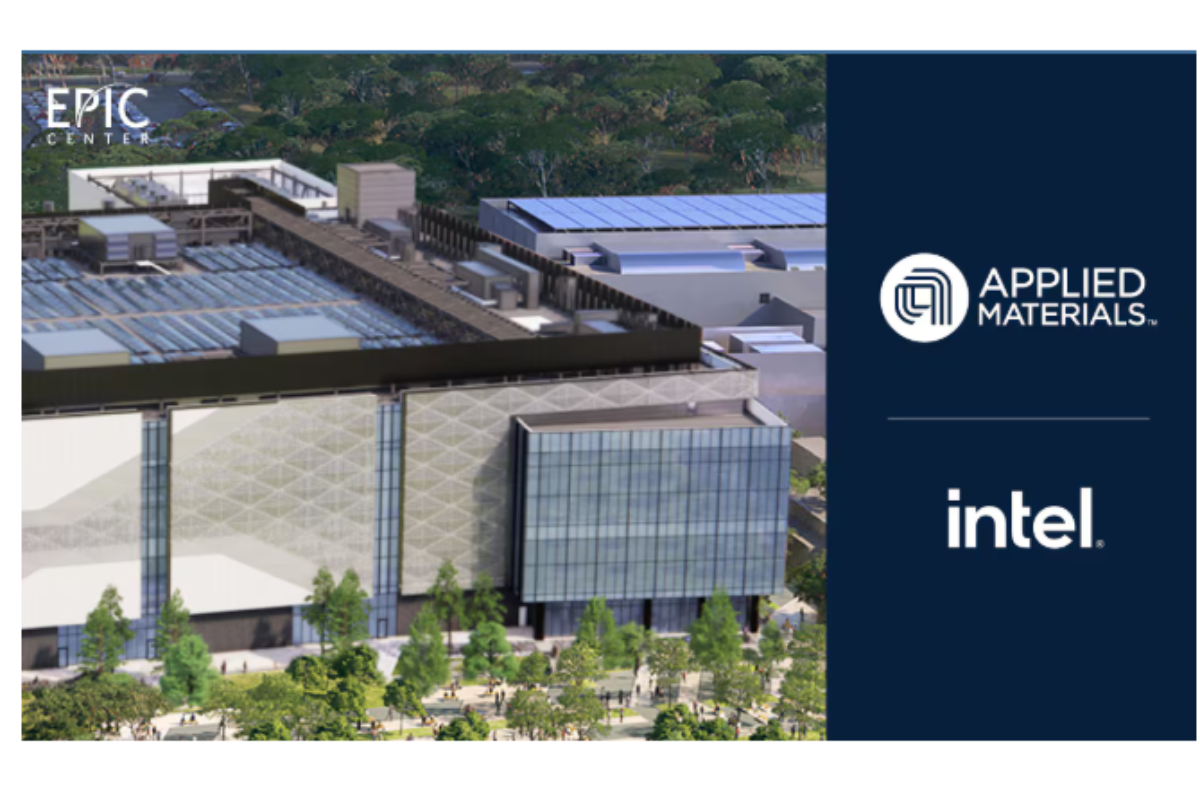
The facility combines Applied Materials’ wafer processing systems with CEA-Leti’s capabilities in evaluating new materials and device validation. The upgraded lab is expected to enhance the chipmaking ecosystem in France by expanding the technology hub in Grenoble, which serves as a center for collaboration among government, academia, and industry. The lab also aligns with Applied Materials’ global EPIC Platform, a model designed to accelerate the commercialization of new chip technologies by leveraging R&D across its global innovation centers.
Aninda Moitra, corporate vice president and general manager of Applied Materials’ ICAPS business, stated that the collaboration builds on a history of partnership to advance specialty chip innovation and commercialization. Sébastian Dauvé, CEO of CEA-Leti, noted that the initial phase of the collaboration addressed materials-engineering challenges, and the expanded focus on energy-efficient solutions for AI data centers aims to meet industrial and societal needs while supporting sustainable growth in France’s semiconductor ecosystem.