ERS electronic announced the opening of its latest demonstration center in Zhubei, Taiwan. This new facility will provide chipmakers and Outsourced Semiconductor Assembly and Test companies in Taiwan with direct access to ERS’s cutting-edge PhotoThermal debonding machine for wafers and panels, the LUM600S1. This strategic move aims to address the increasing demand for panel-level packaging technologies in the region.
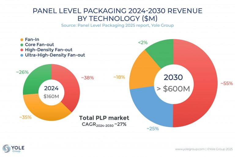
Panel-level packaging is rapidly gaining traction in the semiconductor industry due to its cost advantages and process scalability. According to Dr. Yik Yee Tan, Technology & Market Principal Analyst at Yole Group, the PLP market is expected to grow from $160 million in 2024 to over $600 million by 2030, driven by cost-efficient solutions in advanced packaging.

By 2030, high-density fan-out technology, propelled by Generative AI, is anticipated to dominate the market, capturing more than 50% of the market share. The demand for larger form factors in chiplet and heterogeneous integration is driving the growth of PLP to meet higher density requirements. For large package sizes of approximately 5.5x the reticle size limit, PLP can boost carrier area efficiency by more than 80%, compared to just 45% with Wafer Level Packaging.
ERS electronic has been at the forefront of PLP technology, being one of the first to introduce PLP equipment to the market with the launch of a panel-level debonder in 2018. ERS offers a comprehensive portfolio of semi- and fully-automatic systems, including PhotoThermal debonding machines that enable temporary bonding and debonding processes essential for handling ultra-thin substrates. This capability is critical for high-performance computing and AI applications, such as CoWoS and HBM.

“With the LUM600S1, we are providing a high-yield solution tailored for high-volume manufacturing of complex AI chips. Our Taiwanese customers can now experience firsthand how PhotoThermal Debonding enhances efficiency, scalability, and cost-effectiveness,” said Sébastien Perino, Managing Director of ERS Taiwan.
For more information, please visit https://www.ers-gmbh.com/