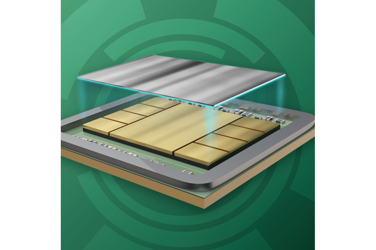

A research team led by National Taiwan University (NTU) has fabricated wafer-scale, single-layer p-type boron carbon nitride (BCN) for potential use in two-dimensional complementary metal–oxide–semiconductor (CMOS) technology. The team reports that the material has high hole mobility.
Two-dimensional semiconductors are being studied for next-generation miniaturized transistors and three-dimensional integration. While research into high-performance n-type 2D semiconductors has advanced, comparable p-type materials remain scarce, and achieving both strong carrier transport and large-area growth has been a challenge.

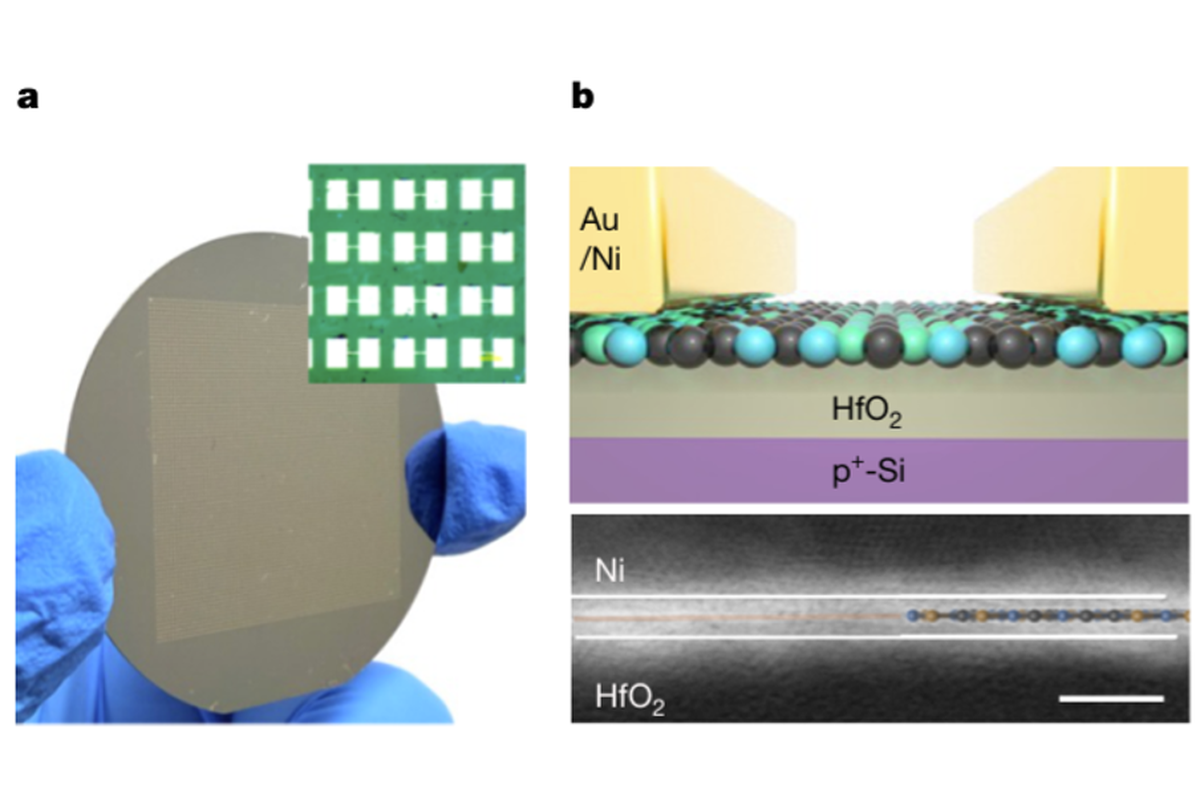
The researchers introduced carbon atoms into the atomic lattice of monolayer boron nitride (BN), changing its electronic states and inducing p-type semiconducting behavior. By controlling the reaction pathways of two precursor molecules, they grew the atomic-scale structure across a two-inch wafer. The team describes this as the first wafer-scale fabrication of BCN.

The study used atomic-resolution electron microscopy, scanning tunneling spectroscopy, first-principles calculations and transistor performance evaluations to examine links among carbon substitution, electronic states and p-type electrical conductivity. The researchers say more precise control of the amount and location of carbon substitution could enable atomic-level engineering of carrier concentration and electronic states in BCN. They also expect the material to be compatible with n-type 2D semiconductors such as molybdenum disulfide (MoS₂) for potential use in complementary electronic circuits.
The research was jointly led by Professor Yi-Chia Chou's team at NTU's Department of Materials Science and Engineering, Professor Vincent Tung's team at the University of Tokyo, and Research Fellow Chun-Wei Pao's team at the Research Center for Applied Sciences, Academia Sinica. The findings were published online in Nature on September 30, 2026 (DOI: 10.1038/s41586-026-11047-9).