

Hanyang University Researchers Develop EF-SCN Method for 2D Semiconductor Crystal Growth
Hanyang University researchers and collaborating institutions have developed etching-flux-mediated single-centred nucleation (EF-SCN), a method for directing where molybdenum disulfide crystals form for two-dimensional electronics. The researchers reported more than 99% single-crystal growth across 400 sites.
Nucleation, when crystals first begin to form, affects where and how they grow. The release says conventional area-selective growth methods cannot reliably control nucleation within designated regions, making it difficult to produce large single crystals and precisely aligned structures for electronic devices.
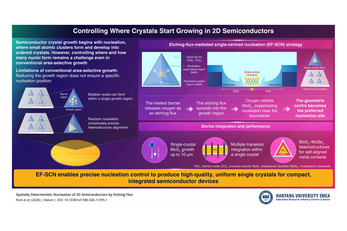
In a study published in Volume 658 of Nature on October 7, 2026, the researchers used metal-organic chemical vapor deposition to grow molybdenum disulfide (MoS2) on patterned substrates. A hafnium oxide (HfO2) barrier around each growth region releases oxygen when heated to 750°C. The oxygen etches material near pattern boundaries, suppressing nucleation there and favoring a single crystal at the center. As growth c...