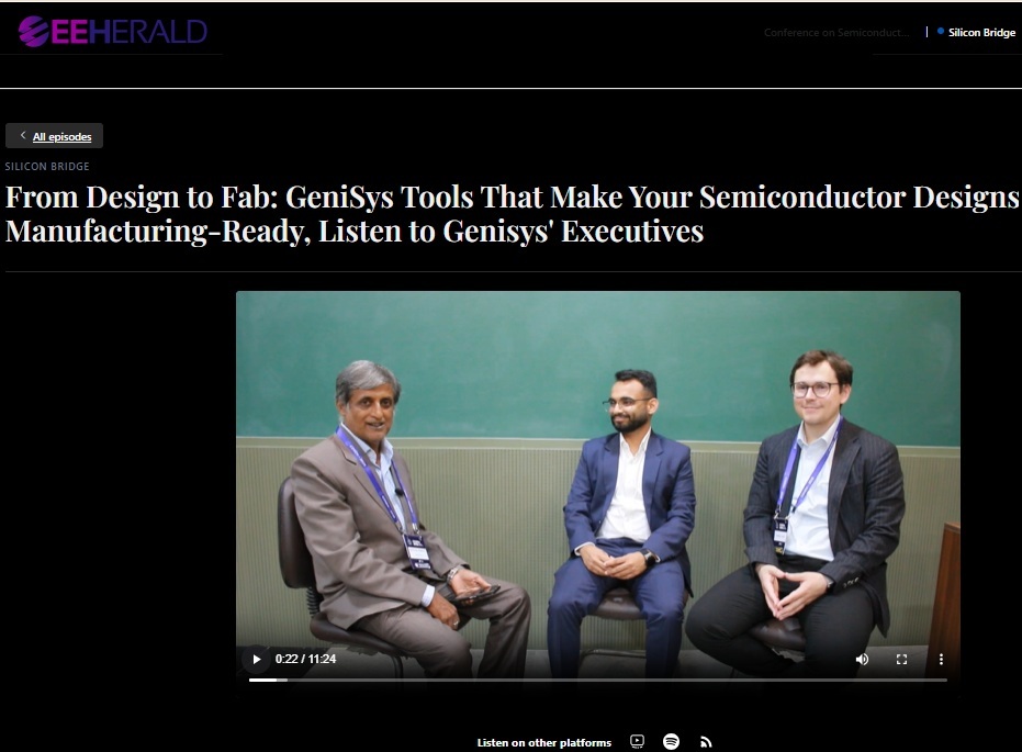
In an interactive talk hosted by Srinivasa Reddy N, Editor of EEHerald, executives from GeniSys GmbH shared insights into the company’s software solutions for advanced semiconductor manufacturing and their relevance to India’s expanding ecosystem of design centers and upcoming fabrication facilities.
Kaustubh and Dmitri, the two executives participating in the discussion, highlighted that while significant progress is underway in India’s semiconductor sector—with numerous design houses and new fabs—critical gaps remain, particularly in the “middle ground of prototyping.” GeniSys, which has operated for nearly two decades, positions its solutions across design, prototyping, and manufacturing stages to address these gaps.
The company’s software works in conjunction with direct writing tools such as electron beam lithography (EBL) and other lithography systems. GeniSys partners with tool manufacturers including Raith, JEOL, Crestec, and Elionix. It already has installations in India and supports the transition from R&D environments, such as those at institutions like IISc, toward production.
Correcting Lithography Effects for Design Accuracy
Kaustubh explained that when designers create files such as GDS files for chip manufacturing, these are typically used in electron beam or laser lithography tools or sent to large fab houses. During the lithography process, deleterious effects can distort intended structures—for example, a designed 100-nanometer waveguide or channel may result in dimensions of 80 nm or 120 nm, compromising the entire design.
GeniSys software corrects for these effects, ensuring the manufactured outcome matches the original design exactly. This makes designs production-ready and machine-readable, directly supporting manufacturability at the nanometer scale.

Supporting the Full Manufacturing Process
Dmitri noted that GeniSys solutions cover multiple stages of the manufacturing process, from design preparation and lithography to simulation (including for packaging), process optimization, stability, and post-production metrology and inspection.
The executives emphasized that the company operates in both R&D and special production environments worldwide. Its presence in India reflects growing investments and expanding semiconductor businesses in the country, which GeniSys views primarily as an opportunity.
Academic and Ecosystem Collaborations
GeniSys maintains close strategic partnerships with major global universities, including Stanford, MIT, Harvard, and Caltech, where it supports prototyping and chip-making activities. The company aims to replicate this model in India, particularly with premier institutions such as CeNSE at the Indian Institute of Science (IISc).
Kaustubh stressed that rapid prototyping at the university level is where novelty and new processes originate. GeniSys has grown alongside its customers over 20 years, continuously developing its software based on direct customer feedback and feature requests for new products and applications. The company recently conducted a local workshop in India, which featured good attendance and productive discussions with students.
Outlook Toward 2030
Looking ahead, Kaustubh observed that while India has focused extensively on the design side—including EDA tools and empowering designers—greater attention is now needed on manufacturing. He encouraged stakeholders to “get their hands dirty” and begin producing more chips.

By 2030 and beyond, GeniSys hopes to deepen collaboration with Indian academic and R&D institutions, which train the next generation of semiconductor professionals. The company also aims to engage with larger fabs emerging in India. GeniSys seeks to replicate the success it has achieved in North America and Europe—markets where it has strong university presence—while noting that Asia, including India, represents a significant opportunity.
Dmitri expressed satisfaction with the company’s participation in India’s semiconductor development, highlighting the cleanroom-appropriate nature of their work and their enthusiasm for contributing to the ecosystem.
The discussion concluded with the host thanking the executives for their insights into GeniSys’s role in enabling accurate, production-ready semiconductor manufacturing in India.