Cadence has announced the launch of the industry’s fastest HBM4 12.8Gbps memory IP solution, designed to meet the growing memory bandwidth demands of SoCs for next-generation AI training and HPC hardware systems. This new solution, compatible with the JEDEC specification JESD270-4, doubles the memory bandwidth compared to the previous HBM3E IP products. 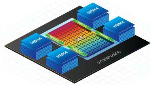
The Cadence HBM4 solution, now available for customer engagements, includes a PHY and controller IP that deliver an industry-leading performance of 12.8Gbps. This solution offers 20% greater power efficiency per bit and 50% better area efficiency while doubling the number of I/Os for higher bandwidth.
Key Features:
High Performance: The HBM4 PHY and controller IP achieve a data rate of 12.8Gbps, exceeding current HBM4 DRAM device speeds by 60%.
Efficiency: The solution provides 20% greater power efficiency per bit and 50% better area efficiency.
High Performance: The HBM4 PHY and controller IP achieve a data rate of 12.8Gbps, exceeding current HBM4 DRAM device speeds by 60%.
Efficiency: The solution provides 20% greater power efficiency per bit and 50% better area efficiency.
Compatibility: Available as a drop-in hardened macro in TSMC N3 and N2 technology nodes, with the controller provided as a soft RTL macro.
Advanced Architecture: Includes RAS and BIST features for optimal data center operations and supports various interposer design implementation options.
“The proliferation of generative and agentic AI applications and the resulting increase in AI workloads demand higher memory bandwidth for greater AI hardware system efficiency without further draining power. Cadence’s HBM4 solution addresses this insatiable need for memory bandwidth by providing the highest performance available at 12.8Gbps while maintaining area and power efficiency—key concerns for AI factories,” said Boyd Phelps, senior vice president and general manager of the Silicon Solutions Group at Cadence.
Cadence’s HBM4 solution includes a reference interposer design validated at 12.8Gbps on a full-featured test chip, LabStation software for rapid SoC post-silicon lab bring-up, and verification with Cadence’s Verification IP for HBM4.
For more information, visit www.cadence.com.