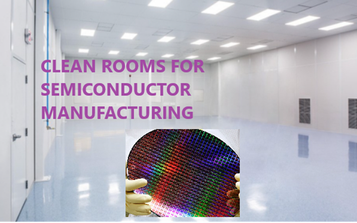
Applied Materials introduced two new chipmaking systems: Centris Spectral SiN ALD and Producer Selectra Mo Etch. The systems are designed for precision materials engineering in high-aspect-ratio 3D structures in logic and memory chips. They are currently in use by leading logic and memory chipmakers for advanced node manufacturing.
The systems address processing challenges in advanced 3D device architectures, including gate-all-around (GAA) transistors and high-layer-count 3D NAND, driven by AI compute demand. As features become deeper and narrower, uniform top-to-bottom material distribution becomes more difficult with conventional processes.
Centris Spectral SiN ALD
The Centris Spectral SiN ALD system uses innovative microwave plasma technology to deliver uniform silicon nitride (SiN) deposition in challenging 3D structures. SiN films are used for surface passivation, dielectric isolation, and patterning spacers. The system deposits high-quality SiN at low temperatures without the tradeoffs of conventional plasma-enhanced methods, such as poor uniformity or ion-induced damage.

Applications include forming high-quality liners for transistor contacts in GAA devices to reduce resistance and capacitance. The system is part of Applied’s Spectral ALD platform, which features a quad reactor design with precision chemical delivery, plasma and thermal processing capabilities, and support for temporal and spatial ALD operations.
Producer Selectra Mo Etch
The Producer Selectra Mo Etch system provides selective removal of molybdenum (Mo) for wordline separation in 3D NAND scaling. As layer counts increase, low-resistance metals like molybdenum require precise isolation to prevent shorts and reduce capacitance. The system uses engineered process control and advanced gas delivery to achieve uniform top-to-bottom etching in high-aspect-ratio features, overcoming limitations of traditional wet etch processes.

It reduces cell-to-cell variability, lowers leakage, and improves data retention. The system has been validated in high-volume manufacturing and expands the Selectra portfolio into advanced metal integration for NAND, DRAM, and foundry-logic applications.
Dr. Prabu Raja, President of the Semiconductor Products Group at Applied Materials, stated: “As the industry pushes the limits of AI computing, the biggest opportunities are increasingly found in materials engineering. From transistor structures to memory stacks, chipmakers need new ways to precisely deposit and selectively remove materials in extremely complex 3D architectures. With our latest deposition and selective etch systems, we are delivering differentiated capabilities that help customers overcome critical scaling barriers and accelerate the next wave of innovation in logic and memory.”
The new systems will be featured at the 2026 IEEE Symposium on VLSI Technology & Circuits. Applied Materials is also hosting a panel discussion on June 16 on the co-optimization of system architectures, logic and memory technologies, advanced packaging, and manufacturing for AI-driven compute.