Design Guide

SoC Design: The Hidden PPA Killer Lurking in Every Clock Tree: Why Buffer Size Still Rules Advanced Node VLSI Chip Design
The role of buffer size in System-on-Chip (SoC) and complex VLSI designs is one of the most critical yet subtle optimization levers available to physical design engineers. Buffers (including inverters used as buffers) are inserted throughout the chip to manage signal integrity, timing, power, are
21 min read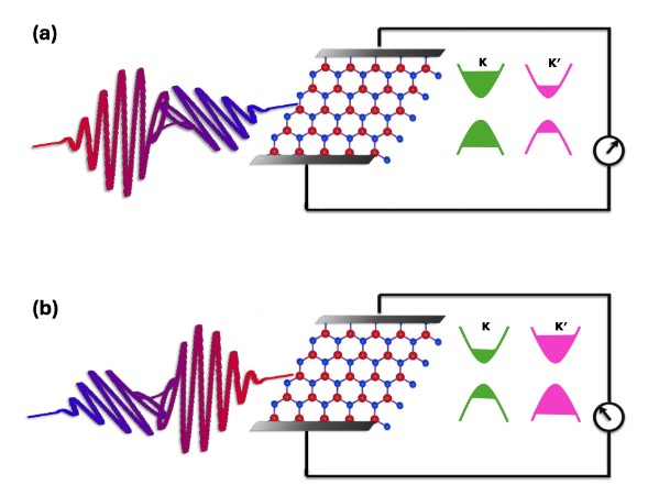
IIT Bombay Researchers Demonstrate Ultrafast Valley Switching in 2D Semiconductors Using Single Linearly Polarized Pulse
Researchers at the Indian Institute of Technology Bombay have developed a method to control and read quantum valley states in atom-thin two-dimensional (2D) semiconductors using a single linearly polarized laser pulse. The study, published in Advanced Optical Materials on December 7, 2025
4 min read
The Importance of Data Sheets in Electronics Design and a Short Practical Guide
In electronics design, the data sheet (or datasheet) is the single most important communication bridge between component manufacturer and engineer. It is far more than a simple product brochure: it serves as a technical specification, an implied warranty, a design reference, and frequently even a
15 min read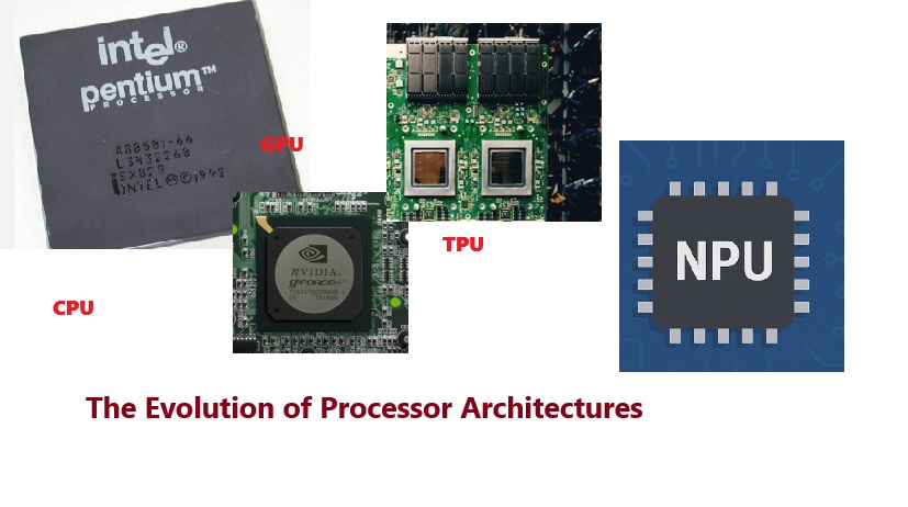
The Evolution of Processor Architectures: From CPUs to GPU, TPU and NPU powered AI Accelerators in 2026
Digital processors have transformed computing over the past five decades, evolving from basic loop like sequential/serial arithmetic and logic processing units to sophisticated vector processing capable parallel processing accelerators powering artificial intelligence. At their
17 min read
Bluetooth Channel Sounding for Distance Measurement and Other Applications
At the Works With event organized by Silicon Labs in Bangalore on October 30, 2025, Vijaya Krishna presented demonstrations and details on the use of Bluetooth channel sounding for distance measurement, along with related technologies including PAWR, Bluetooth mesh, ambient IoT, LE Audio, and upc
9 min read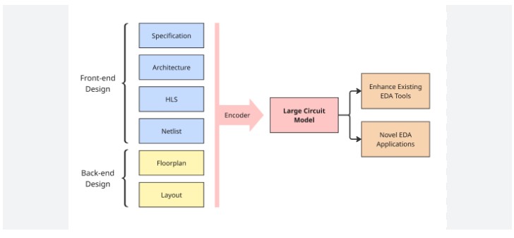
AI EDA tools: AutoChip Leverages Large Language Models for Verilog Module Generation
A new tool, AI VLSI semiconductor design EDA tool AutoChip, has been developed to generate functional Verilog modules from initial design prompts and testbenches using large language models (LLMs). The tool, detailed in a paper accepted for publication in the ACM Transactions on Design Automation
3 min read
The Big Trend in Semiconductor Design: Unifying Compute and Memory
In the human brain, computing and memory reside in close proximity ensuring near instant processing. In contrast, computer systems keep the computing and memory away, causing access delays and reduced performance. To achieve human-like efficiency, processors and memory must be t
14 min read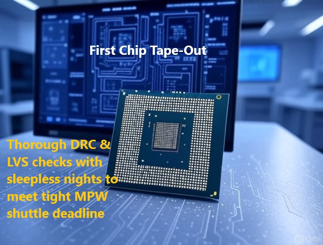
First Semiconductor chip Tape-Out: IC Product Startup’s Survival Test
After months of schematics, simulations, and DRC and LVS checking sleepless nights, a product VLSI startup’s first tape-out marks a key milestone in the tough world of semiconductor design. This is the moment when a chip design transitions from digital blueprints to physical silicon, a proc
6 min read
2nm Chip Design Challenges: Signal Parasitics Impact Performance and Power Efficiency
At deep nodes such as 2nm, signal parasitics create bigger challenges. The electrical characteristics like resistance, capacitance, and inductance pose significant challenges to chip performance, power efficiency, and design complexity. These parasitic effects, arising from the physical layout of
6 min read
Module 3a: Introduction to VLSI and Digital Design
For young electronics engineering graduates in India, a career in VLSI design offers excellent long-term growth and the satisfaction of working in a core electronics field. However, VLSI design demands a stro
36 min read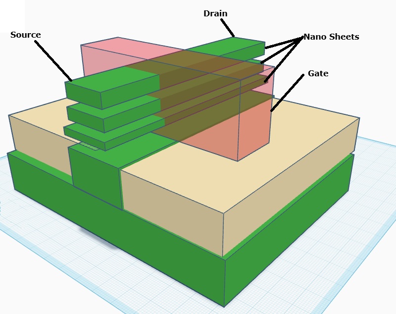
FinFET vs. GAAFET vs. Nanosheet FET: A TCAD Modeling and Behavioral Analysis
The relentless pursuit of Moore's Law has driven transistor architectures from planar MOSFETs to sophisticated 3D structures. FinFETs marked a significant advancement, but as scaling approaches sub-5nm nodes, Gate-All-Around FETs (GAAFETs), particularly Nanosheet FETs (NS-FETs or MBCFETs), have e
11 min read
Module 2b: Introduction to VLSI and Digital Design
For young electronics engineering graduates in India, a career in VLSI design offers excellent long-term growth and the satisfaction of working in a core electronics field. However, VLSI design demands a stro
63 min read
Our Editors dive into topical news, new products, and discuss the shifting architecture of the global semiconductor industry.
▶ Podcast