Applied Materials launched three new semiconductor manufacturing systems designed to improve the energy-efficient performance of logic chips at 2nm process nodes and beyond. These systems target enhancements to Gate-All-Around (GAA) transistors and associated wiring, which are key elements in the production of advanced chips used for AI applications.
The transition to GAA transistors represents a significant shift in the industry, enabling more energy-efficient computing for higher-performance AI chips. As 2nm-class GAA chips move toward volume production in 2026, Applied Materials has developed these tools to address atomic-scale challenges in transistor structures and contacts.
The Applied Producer Viva radical treatment system provides atomic-level precision in smoothing the surfaces of GAA silicon nanosheets. These nanosheets, which are a few nanometers wide and stacked horizontally, require uniform and pristine surfaces to optimize electron mobility, which affects transistor switching speed and energy efficiency. The Viva system uses a patented architecture with a remote plasma source to generate ultra-pure neutral radicals, avoiding damage from high-energy ions. This enables uniform treatment in complex transistor structures. The system is being adopted by leading logic chipmakers for 2nm and smaller nodes. It also has applications in logic and memory, including reducing resistance in copper wires when combined with thermal annealing.

The Centris Sym3 Z Magnum etch system is the latest in the Sym3 Z family, which previously introduced pulsed voltage technology for high-aspect-ratio features in GAA transistors. The new system incorporates second-generation pulsed voltage technology (PVT2), allowing independent control of ion angle and energy. This results in precise 3D trench profiles with uniform depth, straight sidewalls, and flat bottoms, improving silicon nanosheet uniformity, switching speed, and epitaxial quality. The system supports both advanced logic and memory technologies, such as DRAM and high-bandwidth memory. It has seen adoption among leading chipmakers.
The Centris Spectral atomic layer deposition (ALD) system enables selective deposition of monocrystalline molybdenum to replace traditional tungsten in transistor contacts. At sub-2nm scales, thinner contacts increase resistance, creating performance bottlenecks. Molybdenum allows thinner structures while maintaining efficient electron flow. The system reduces contact resistance by up to 15% compared to the current benchmark using the Applied Endura Volta Selective Tungsten system. These contacts connect transistors to the copper wiring network. The Spectral platform features a quad reactor design with advanced chemical delivery and processing options. It is being adopted by leading logic chipmakers at 2nm and below nodes.

The new systems are currently in use by multiple leading foundry-logic manufacturers. Applied Materials states that the combined improvements from these tools contribute significantly to the energy-efficient performance gains in GAA node transitions.
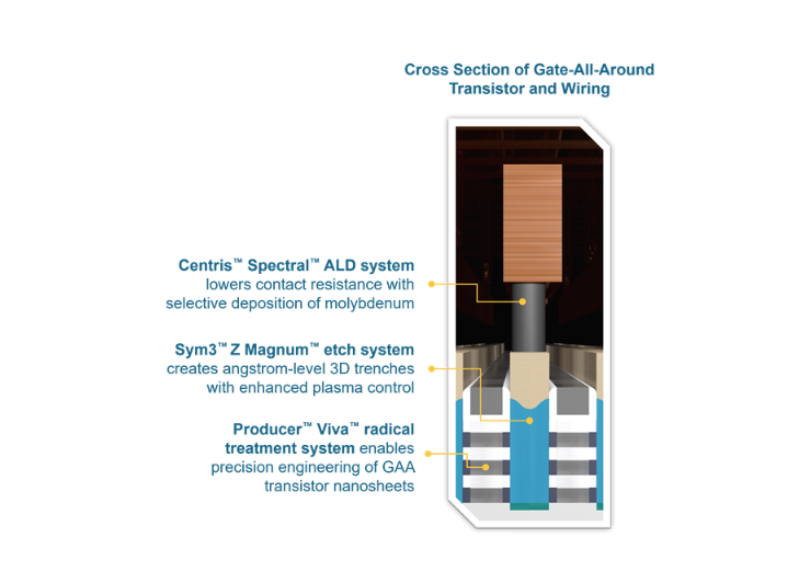
A cross-sectional image of a Gate-All-Around transistor and wiring