The global semiconductor device market is estimated to reach around $800 billion in sales in 2025 with a growth of more than 25% compared to 2024 and if the same trend continues it is projected to exceed 900 billion in 2026, as per latest study be EMITT Solutions. This new trend of growth is driven almost entirely by AI infrastructure, high-bandwidth memory (HBM), advanced logic nodes, data-center expansion, and automotive electrification.
Geopolitical diversification efforts (U.S. CHIPS Act, EU Chips Act, China's push, India Semiconductor Mission, Japan subsidies, Vietnam and Malaysia playing important role) continue to accelerate in Asia and outside Asia, yet Taiwan, South Korea, China, and Japan still dominate advanced-node (≤7 nm) logic and high-end memory production. China leads mature-node expansion, Southeast Asia (especially Malaysia) dominates assembly, test & packaging (ATP / OSAT), and the U.S., Europe, Israel, and are scaling domestic capabilities. India is seeing unprecedented growth in manufacturing, where India will start exporting packaged chips in year 2026.
This top 20 ranking of semiconductor manufacturing and design blends:
- Current manufacturing capacity share & advanced technology leadership.
- Physical fab scale & investment momentum (announced projects, wafer starts)
- Design / R&D / IP density
- Ecosystem maturity & supply-chain criticality
- Near-term 2026–2030 impact on AI, automotive, and resilience
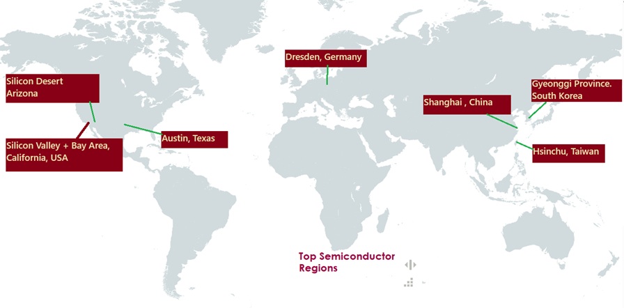
1. Hsinchu + Tainan Science Parks, Taiwan
Originated in the 1980s via ITRI spin-offs and UMC/TSMC founding; became the foundry capital by the mid-2000s through relentless node scaling. TSMC’s dominance in ≤3 nm logic and advanced packaging (CoWoS) solidified unmatched density. In 2026 it holds majority of global advanced-node capacity. Future depends on successful N2/N1 ramp and managing geopolitical/water risks.
2. Gyeonggi Province (Pyeongtaek, Yongin, Icheon), South Korea
Emerged in the 1980s–1990s as Samsung and SK hynix built memory giants. Pyeongtaek became the world’s largest single campus complex. Dominates HBM and high-end DRAM/NAND critical for AI. In 2026, HBM supply remains the primary AI GPU bottleneck. Future trajectory centers on massive Yongin expansion and sustaining memory leadership amid competition.
3. Silicon Valley + Bay Area, California, USA
Birthplace of the industry since the 1950s–1960s transistor era; evolved into the global design/IP hub by the 1990s–2000s fabless model. Now hosts Nvidia, AMD, Broadcom, and equipment leaders. Captures ~50% of industry revenue through architecture dominance. In 2026, AI chip design drives value. Future hinges on maintaining innovation edge and talent pool.
4. Silicon Desert (Phoenix / Chandler), Arizona, USA
Intel roots date to the 1970s–1980s; transformed post-2020 via CHIPS Act and TSMC’s entry. Rapid shift to advanced-node manufacturing outside Asia. TSMC’s $65B+ GIGAFAB cluster targets N4/N3 ramp. In 2026, fastest U.S. growth area. Future: major non-Asian advanced logic center by late decade.
5. Silicon Hills + Taylor, Austin Area, Texas, USA
Began with AMD/IBM in the 1980s–1990s; exploded with Samsung’s 300 mm fab in the 2000s. Now blends logic, memory, and systems integration. Massive Taylor site and state incentives fuel momentum. In 2026, strong CHIPS Act beneficiary. Future: large-scale capacity addition with design synergy.

6. Silicon Saxony (Dresden), Germany
Revived post-reunification in the 1990s with GlobalFoundries/Infineon investments. Became Europe’s leading advanced/specialty cluster. New Bosch AI fab adds momentum. In 2026, key automotive/power IC hub. Future: EU Chips Act expansion into more specialty and mature nodes.
7. Shanghai / Yangtze River Delta, China
Grew rapidly in the 2000s–2010s via SMIC/Hua Hong foundries and state support. Became mature-node powerhouse (14–28 nm & legacy). High utilization despite restrictions. In 2026, drives nearly half of planned global wafer additions. Future: continued mature-node dominance and pricing pressure.
8. Tokyo–Kanto + Kumamoto / Kyushu, Japan
Equipment/materials leader since the 1980s–1990s (Tokyo Electron, Shin-Etsu). Declined in logic but revived via Rapidus 2 nm and TSMC Kumamoto JV. In 2026, strong sensors/equipment role. Future: government-backed logic resurgence and advanced packaging.
9. Singapore
Became Southeast Asian wafer fab hub in the 1990s–2000s with Micron, GlobalFoundries, UMC. Evolved into advanced packaging/OSAT center. In 2026, key regional equipment/R&D node. Future: sustained ATP strength and design growth.
10. Penang + Kulim, Malaysia
Emerged as electronics assembly hub in the 1970s (“Silicon Valley of the East”). Evolved into world’s largest ATP/OSAT cluster (around 13% global share) post-2000. Intel/Infineon/Micron expansions since 2022 cemented advanced packaging. In 2026, back-end diversification leader. Future: climb into more design/equipment.
11. Bengaluru, India
Rose in the 1990s–2000s as India’s IT hub; became dominant semiconductor design cluster by 2010s with AMD, Intel, Qualcomm centers. Over 300 firms now. In 2026, massive AI/automotive/analog talent pool. Future: global IP powerhouse with growing R&D scale. Along with product companies Bengalure also have big offices of EDA and Semiconductor equipment makers.
12. Greater Bay Area (Shenzhen), China
Exploded in the 2000s–2010s as fabless/systems hub (Huawei HiSilicon, DJI). Grew mature-node fabs amid self-sufficiency push. In 2026, dense consumer/AI ecosystem. Future: continued fabless strength and electronics product design strength.
13. Gujarat (Dholera + Sanand), India
Launched under 2021 India Semiconductor Mission. Micron ATMP began ramp early 2026; Tata-PSMC 300 mm fab targets late 2027/early 2028 first chips. In 2026, flagship emerging hub. Future: front-end/back-end growth with supplier ecosystem.

14. Israel (Kiryat Gat)
Intel fab established in the 1980s–1990s; grew into advanced-node site plus Mobileye/Habana design strength. In 2026, significant fab + innovation density. Future: sustained advanced manufacturing and IP leadership.
15. New York / Hudson Valley, USA
Micron megafab project announced 2022; construction progressing under CHIPS Act. Focus on advanced memory scale-up. In 2026, major upcoming memory addition. Future: key U.S. memory capacity contributor by late decade.
16. Ohio (Silicon Heartland), USA
Intel multi-fab plan launched 2022; construction advancing despite timeline adjustments. In 2026, large-scale future capacity site. Future: significant long-term U.S. logic/memory expansion.
17. Hanoi / Bac Ninh area, Vietnam
Grew as Samsung/Intel ATP hub in the 2010s. Viettel indigenous fab trials ~2027. In 2026, fast-growing back-end + early front-end ambition. Future: Southeast Asia’s next ATP wave.
18. Leixlip, Ireland
Intel Fab 34 (Intel 4 / EUV) reached volume production 2023. Europe’s most advanced single site. In 2026, key EU advanced-node anchor. Future: sustained Intel European capacity role.
19. Hyderabad, India
Emerged as secondary design/embedded hub in the 2000s–2010s (AMD, Intel, Qualcomm). Complements Bengaluru. In 2026, growing talent pool. Future: design diversification support.
20. Thailand (various sites)
Developed ATP/OSAT presence in the 2000s–2010s (Delta, Hana). In 2026, emerging back-end player. Future: lower-tier ATP/OSAT growth amid regional diversification.
PS: Edited one sentence in the above article dated 11th Feb 2026 for some corrections.