Avicena, known for its microLED-based optical interconnect technology, announced it will demonstrate what it describes as the industry's first connectorized microLED optical interconnect. The new LightBundle eKit implementation combines Avicena's high-density, laser-free microLED transceiver technology with an inline, detachable optical interface, offering a practical way to assemble, test, service, and upgrade optical connectivity in next-generation AI systems.
Avicena will demonstrate the connectorized LightBundle eKit at Stand 1365 during ECOC Exhibition 2026, taking place September 21-23 at the Palacio de Ferias y Congresos de Málaga in Spain.
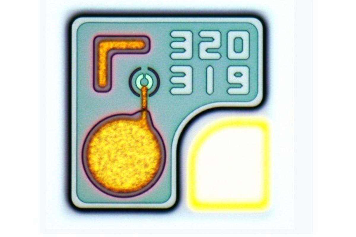
The announcement builds on Avicena's recent shipment of what it describes as the world's first 1 Tbps microLED optical interconnect evaluation kits. Those systems incorporate as many as 335 independent microLED data channels, each operating at up to 3 Gbps, coupled through Avicena's multicore fiber technology to integrated photodetector arrays, which convert the optical signals back into electrical ones. The new connector uses an industry-standard MPO form factor paired with a ferrule, the small component that aligns fiber optic connections, optimized specifically for multicore fiber bundles.
Bringing Serviceable Optical Connectivity Closer to the Silicon
AI systems require rapidly increasing bandwidth between accelerator chips (XPUs), memory, network interfaces, and switch fabrics. As these systems scale up, conventional copper interconnects face growing limitations around physical reach, routing density, signal integrity, and energy efficiency.
Optical connections can overcome copper's reach limitations, but conventional optical technologies based on lasers and silicon photonics can introduce significant challenges around power consumption, heat, cost, packaging, and reliability, particularly when optical connectivity needs to sit close to high-performance compute and memory chips.
LightBundle replaces lasers with dense arrays of microLED transmitters, coupled through multicore fiber to integrated photodetector arrays. Its "wide-and-slow" architecture spreads bandwidth across hundreds of low-power optical channels, achieving high total throughput without requiring the extremely high per-channel speeds and complex signal processing that conventional optical links typically need.
The new connectorized version adds the modularity needed for practical system integration. A detachable optical interface can simplify system assembly, allow independent testing of electronic and optical subsystems, improve serviceability in the field, and support flexible routing between chip packages, circuit boards, server trays, and racks.
Marco Chisari, CEO of Avicena, said introducing the world's first connectorized microLED optical interconnect marks an important step in moving microLED connectivity from a breakthrough technology into a deployable platform for AI infrastructure. He said that following the shipment of Avicena's 1 Tbps LightBundle evaluation kits, the company is now demonstrating how the same underlying architecture can be implemented with the modularity and serviceability system manufacturers require. He said this advancement further extends Avicena's leadership and brings energy-efficient, terabit-class optical connectivity closer to broad deployment across XPU-to-XPU, XPU-to-memory, XPU-to-CPU, and XPU-to-switch applications.
Designed for AI Scale-In and Scale-Up
LightBundle is designed to support optical connectivity across both "scale-in" architectures, meaning connections within a single system, and "scale-up" architectures spanning multiple systems, including die-to-die and die-to-memory connectivity within or between chip packages; XPU-to-XPU and XPU-to-CPU interconnects; XPU-to-memory connections and memory-disaggregation architectures, where memory resources are pooled and shared rather than tied to individual processors; XPU-to-switch and network interface card (NIC)-to-switch connectivity; and board-to-board, tray-to-tray, and rack-to-rack links.
The platform's integrated microLED and photodetector arrays are designed for low power operation, high bandwidth density, reliable performance at elevated temperatures, and flexible reach beyond the practical limits of high-speed copper connections.
Unlike laser-based architectures, LightBundle doesn't require external lasers, wavelength stabilization, optical modulators, or complex wavelength-division multiplexing, a technique for sending multiple signals over different light wavelengths on the same fiber. The architecture is also designed to work with a broad range of semiconductor manufacturing processes and packaging approaches, letting optical connectivity be placed closer to compute, memory, and switching silicon.
Ben Bajarin, CEO and principal analyst at Creative Strategies, said adopting a new interconnect technology requires customers to understand how it will actually be manufactured, assembled, and serviced within their systems. He said Avicena's work on a connectorized interface addresses an important part of that challenge and represents a necessary step toward making microLED interconnect technology practical for AI infrastructure, where customers have differing requirements for bandwidth, power, and system design.
Live Demonstration at ECOC 2026
At ECOC 2026, Avicena will demonstrate a live, inline connectorized LightBundle eKit link operating between microLED transmitter and integrated photodetector arrays. The demonstration will highlight detaching and reconnecting the optical interface, real-time data transmission across the connectorized link, high-density parallel connectivity through multicore fiber, link performance and bit-error-rate monitoring, compact fiber routing suited to space-constrained AI systems, and reliable operation without lasers or optical modulators.
Attendees can see the demonstration and meet the Avicena team at Stand 1365 during ECOC Exhibition 2026, September 21-23, at FYCMA in Málaga, Spain.
Avicena is currently engaging with hyperscalers, AI accelerator companies, memory manufacturers, networking companies, system OEMs, and packaging partners to evaluate LightBundle implementations for future AI infrastructure.