OTC, a subsidiary of the OKI Group, has announced a development in PCB technology. The company has successfully created a 124-layer PCB for wafer inspection equipment, designed to support next-generation high bandwidth memory used in AI semiconductors.This innovation represents a significant advancement over the previous 108-layer designs, achieving a 15% increase in the number of layers.
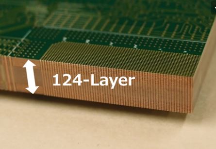
Figure: Cross-section of a 124-layer PCB
OTC aims to establish mass production technology by October 2025 at its Joetsu Plant in Niigata Prefecture, leveraging its extensive experience and advanced capabilities in high multilayer, high-precision, large-format PCBs for semiconductor inspection equipment.
ADVERTISEMENT

As AI processing demands continue to grow, the need for rapid data transmission between GPUs and memory becomes increasingly critical.HBM, with its stacked DRAM structure, requires ultra-thin and precise wafer fabrication. The new 124-layer PCB technology developed by OTC addresses these needs by providing higher performance and quality in inspection equipment.
The latest semiconductors process an enormous number of signals, necessitating increased density and more layers on PCBs used in inspection equipment. Despite the constraints limiting PCB thickness to 7.6 mm, OTC has overcome the previous 108-layer limit by developing ultra-thin materials and tools, along with a proprietary automatic transport system for ultra-thin materials. This has enabled the successful creation of a 124-layer PCB with the same board thickness.
ADVERTISEMENT

The development of this new PCB technology aligns with OKI's commitment to addressing future growth areas, including AI semiconductors, aerospace, defense, robotics, and next-generation communications.
For more information, visit https://www.oki.com/global