CMOS qubits offer a promising approach to scalable quantum computing by integrating quantum bit functionality into standard semiconductor fabrication processes. Electron beam lithography (EBL) is a highly precise method for fabricating these qubits, achieving the sub-22nm resolution required for quantum dot structures and gate electrodes. Below is a step-by-step overview of fabricating CMOS-compatible qubits using EBL:
1. Substrate Preparation
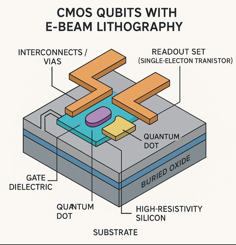
Start with a high-resistivity silicon wafer, typically silicon-on-insulator (SOI), featuring a thin top silicon layer (10–30 nm) and a buried oxide layer (~100 nm). This configuration isolates the active area and minimizes parasitic capacitance.
2. Gate Dielectric Deposition
Deposit a high-k dielectric layer, such as HfO₂ or Al₂O₃, using atomic layer deposition (ALD) to ensure excellent electrostatic control and minimal leakage. The layer thickness is typically 3–5 nm for quantum dot applications.
3. E-Beam Lithography for Gate Patterning
Apply a high-resolution e-beam resist, such as ZEP520A or PMMA, and expose quantum dot gate patterns using EBL at 100 keV to achieve 22nm or better resolution. Key structures to define include:
Quantum dot confinement gates
Barrier gates
Plunger gates
Readout single-electron transistor (SET) or quantum point contact (QPC) gates

Precise alignment and proximity effect correction are essential for multi-layer designs.
4. Metal Gate Deposition and Lift-Off
After resist development, deposit metal gates, typically Ti/Pd or Ti/Au, via e-beam evaporation. The lift-off process removes the resist, leaving patterned gate electrodes.
5. Interconnects and Vias
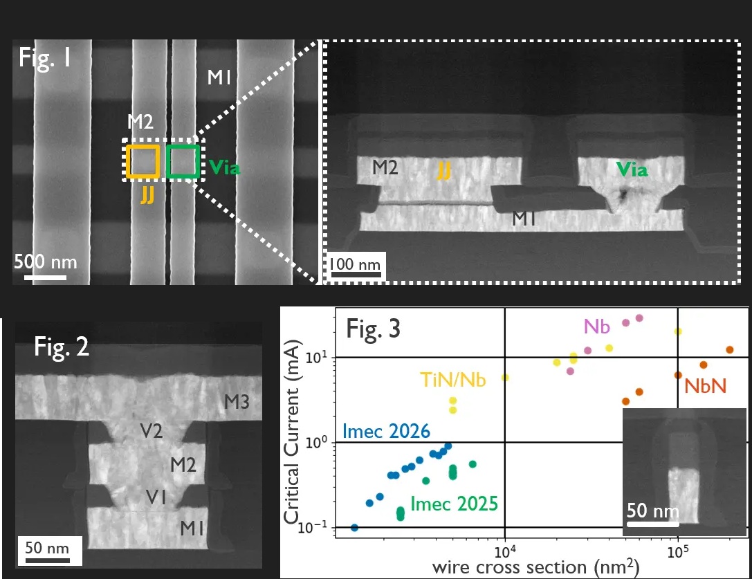
Employ dual-damascene or damascene processes with chemical-mechanical polishing (CMP) to create vias and interconnects linking to CMOS control circuits. Use low-k dielectrics between metal layers to minimize cross-talk.
6. Qubit Initialization Structures
Form single-electron transistors (SETs) or quantum point contacts (QPCs) adjacent to the quantum dots to enable charge sensing, crucial for spin or charge readout of qubit states.
7. Low-Temperature Packaging
After fabrication, wire-bond the chip to a quantum-compatible package and cool it to 10–100 mK in a dilution refrigerator. This temperature range supports electron spin or charge localization and quantum control.
8. Qubit Characterization
Test quantum operations—initialization, manipulation, and readout—using microwave pulses and DC biasing, monitored through SETs or RF reflectometry.
Summary
By utilizing the ultra-precise resolution of electron beam lithography and established CMOS process flows, scalable silicon-based qubits can be fabricated for integration into quantum-classical hybrid chips. EBL at the 22nm node enables precise quantum dot definition, providing the control and reproducibility required for multi-qubit quantum processors, particularly when paired with cryo-CMOS readout electronics.
Author: Marmik Bhat
Founder Monk9 Tech