Chiplets are small, modular semiconductor dies that can be interconnected to form complete systems, offering a new paradigm in chip design as traditional scaling (Moore's Law) becomes economically challenging. This heterogenous integration of chiplets deliver cost savings, faster time-to-market, and greater flexibility compared to monolithic large-die size single SoC chip designs integrating all functions.
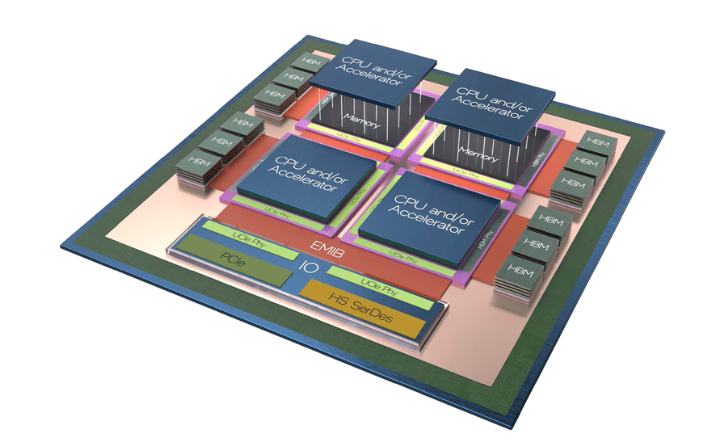
Pic Source: Intel
Key Benefits of Chiplets
- Cost Savings
Smaller chiplets improve manufacturing yields, as defects are less likely on smaller dies, reducing waste and costs.
Mixing process nodes allows cost-effective use of older, cheaper nodes for less demanding functions, while reserving advanced nodes for performance-critical components.
Example: A heterogeneous system might use a mature 28nm node for analog functions and a 5nm node for high-performance digital logic. - Faster Time-to-Market
Chiplets can be designed, tested, and validated independently, speeding up development cycles.
Reusing chiplets across products minimizes redundant design efforts, as seen in AMD’s Ryzen processors, which leverage modular CPU core chiplets. - Flexibility
Chiplets enable a "Lego-like" approach, allowing designers to mix and match dies from various vendors to create tailored systems for specific applications, such as AI accelerators or data center CPUs.
Challenges in Adoption
- Standardization
The absence of universal chiplet interface standards complicates interoperability. Open standards like Bunch of Wires (BoW) and Universal Chiplet Interconnect Express (UCIe) aim to address this, but adoption varies.
Example: BoW offers flexibility but requires coordination for compatibility, while UCIe supports plug-and-play with PCIe and CXL protocols. - Testing
Ensuring chiplets function together requires complex, multi-stage testing (e.g., wafer probe, Known Good Die (KGD), and final system tests), increasing time and cost.
Design for Testability (DFT) techniques like At-speed Scan and Memory BIST target test costs below 20% of die cost. - Packaging
High-performance chiplet systems demand advanced packaging (e.g., silicon interposers, hybrid bonding), which is costlier than standard organic substrates used in lower-end applications.
Current Applications
Chiplets are widely adopted in high-performance computing (HPC):
AMD Ryzen CPUs: Use multiple CPU core chiplets for scalability.
Intel Ponte Vecchio: Integrates compute and memory chiplets for GPUs.
NVIDIA GPUs: Emerging chiplet designs (e.g., Blackwell GB100) enhance performance.
Startups like Ventana and D-Matrix leverage chiplets for data center and AI solutions.
Technical Aspects: How Chiplets Work
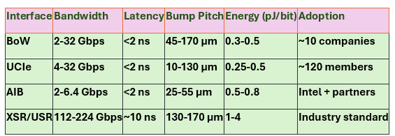
Die-to-Die (D2D) Interfaces
Chiplets communicate via D2D interfaces, critical for bandwidth and latency:
BoW: Open-source, flexible (2-32 Gbps), suited for AI and automotive.
UCIe: Broad industry support (120+ members), optimized for large data loads (4-32 Gbps).
AIB: Intel’s open-source standard, low latency (<2 ns), used in aerospace.
XSR/USR SerDes: High-speed (112-224 Gbps), common in optical networking.

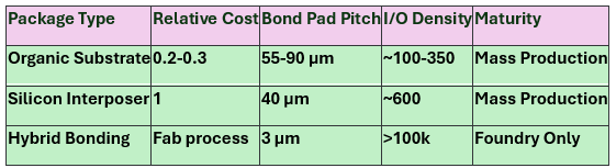
Packaging Technologies
Packaging connects chiplets and impacts cost and performance:
Organic Substrates: Low-cost (relative cost 0.2-0.3), 55-90 μm pitch, mass-produced.
Silicon Interposer: High-density (600 I/O/mm²), costly (relative cost 1), used in HPC.
Hybrid Bonding: Ultra-fine pitch (<10 μm), expensive, foundry-only (e.g., TSMC, Intel).

Economic Advantages:
Yield Improvement
Smaller dies increase usable chips per wafer, offsetting higher packaging costs in large-die, cutting-edge node designs (e.g., 5nm).
- Mixed Process Nodes
Older nodes reduce design and wafer costs for non-critical functions, balancing overall system cost. - Faster Development
Reusing chiplets cuts non-recurring engineering (NRE) costs and accelerates revenue by reaching markets sooner. A McKinsey study notes a 6-month delay can slash profits by 33%, versus 3.5% for 50% higher development costs with timely release.
Sustainability Benefits
Chiplets enhance sustainability by:
Reusing designs, reducing new manufacturing needs.
Extending older process nodes’ lifespans, lowering resource use and carbon footprint.
Future Outlook
Market Growth: Projected to rise from $48 billion (2024) to $204 billion (2032), per Yole.
Open Chiplet Marketplace: Standards like UCIe and BoW could enable off-the-shelf chiplet purchases, though challenges in interoperability, packaging availability, and supply chain persist.
Standardization Efforts: The Chiplet Design Exchange (CDX) proposes models (e.g., thermal, power) and data formats (CDXML) to streamline integration.