
OSAT
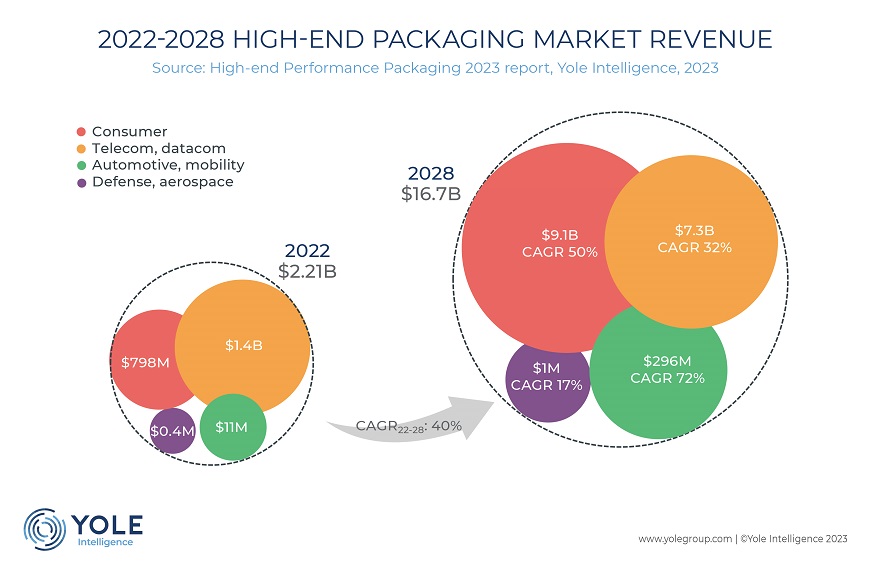
Yole: High-end semiconductor packaging market is $2.2B in 2022, to reach $16 B by 2028
Yole reported that the high-end packaging market was worth US$2.2 billion in 2022 and is expected to reach over US$16 billion by 2028, with a CAGR2022-2028 of 40%. The growth is driven by the industry trend of reducing interconnection pitch. Big players like Intel, TSMC, and Samsung have successf
2 min read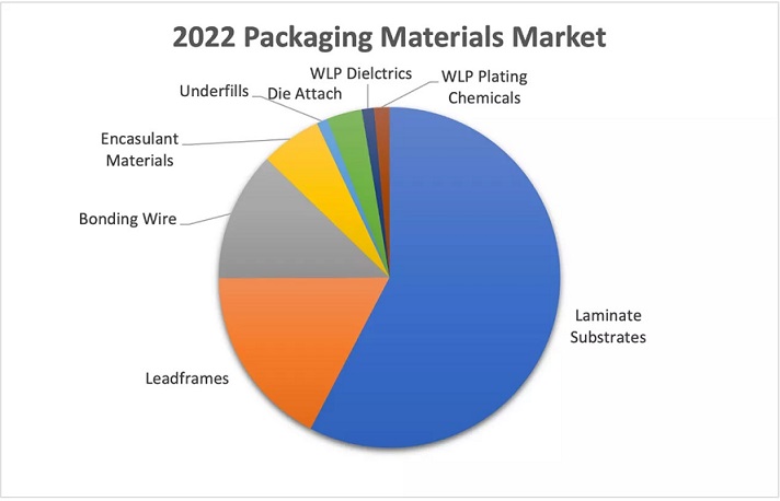
Global Semiconductor Packaging Materials Market to Near $30 Billion by 2027
Powered by strong demand for new electronics innovations, the global semiconductor packaging materials market is expected to reach US$29.8 billion by 2027, a compound annual growth rate (CAGR) of 2.7% from the US$26.1 billion in revenue it logged in 2022, SEMI, TECHCET and TechSearch International a
3 min read
Faster packaging design solutions from Cadence
Cadence has announced its new software which can reduce silicon die to package connect planning time from weeks to few days. Cadence has built this solution using its own technology called OrbitIO, where iterations between silicon and package design teams are reduced and also, time to converge on t
2 min readFine-pitch copper bumps packaging for Arria 10 FPGAs
TSMC’s patented, fine-pitch copper bump-based packaging technology is used in Altera’s 20 nm Arria10 FPGAs and SoCs. Fine-pitch copper bumps are expected to offer better quality and reliability than standard copper bumping solutions. Altera also says the package provides excellent bump joint
1 min readSTS Semiconductor and Invensas partner on BVA chip packaging solution
Invensas and STS Semiconductor & Telecommunications Co. Ltd. have entered into an agreement to validate high volume manufacturing capability for Invensas' Bond Via Array (BVA) tech, a Package-on-Package (PoP) technology for System on Chip (SOC) and memory integration in mobile devices. Called a
2 min readASE partners with Inotera to strengthen SiP packaging capabilities
Advanced Semiconductor Engineering (ASE) is partnering with Inotera Memories to strengthen ASE’s System-in-Package (SiP) capabilities. Inotera to provide manufacturing services for silicon interposer, an interconnect device on silicon wafer for 2.5D IC solutions. Together with ASE’s electro
2 min readeSilicon adds packaging services to its online multi-project wafer quote system
eSilicon, a semiconductor company supporting first-time-right ASICs and ASSPs manufacturing for fables companies has announced the addition of package services to its automated, instant online quote system for multi-project wafer (MPW) shuttles. The service, accessed through user-friendly web or sma
3 min readEvent summary of European Microelectronics and Packaging Conference
The 19th European Microelectronics and Packaging Conference at Grenoble’s World Trade Center in September drew more than 450 attendees from around the world, which was one the biggest crowds in Europe for the event in recent years. EMPC 2013, which also set a record of 60 exhibitors for the Europ
2 min readRFMD completes expansion of its packaging facility in China
RFMD has announced completion of expansion of its test, tape and reel, and assembly facility, located in Beijing, China. In addition to newly qualified internal assembly capacity for power amplifiers (PAs), switch-based products, and antenna control solutions, RFMD is also qualifying advanced fl
1 min readTaiwan's semiconductor packaging industry to benefit from 2.5/3D technologies
SEMI says design tools, manufacturing, packaging and testing solutions for 2.5D-IC process are available this year, and the most important issue is how to improve its throughput to enable 2.5D-IC mass production in 2014. Taiwan is said to benefit from the growth of three-dimensional semiconducto
4 min readSTATS ChipPAC’s latest chip packaging supports 2.5 and 3D fabrication
STATS ChipPAC has expanded Wafer Level Ball Grid Array (eWLB) packaging options to include interposer technology, flip chip interconnect and complex 3D System-in-Package configuration of semiconductor ICs. STATS ChipPAC explains the advancement of silicon scaling to 14 nanometer (nm) in support o
2 min readRudolph acquires NanoPhotonics to enhance position in advanced packaging market
Rudolph Technologies, Inc. has announced that it has acquired the assets of NanoPhotonics GmbH, Mainz, Germany. The addition of NanoPhotonics’ inspection technology and its intellectual property portfolio is to strengthen Rudolph’s presence in the advanced packaging market. Paul F. McLaughlin, ch
4 min read
Our Editors dive into topical news, new products, and discuss the shifting architecture of the global semiconductor industry.
▶ Podcast