CEA-Leti Reports 1 μm Pitch D2W Hybrid Bonding Technology for 3D Semiconductor IC Packaging at ECTC 2026
CEA-Leti has demonstrated a functional test vehicle that uses die-to-wafer (D2W) hybrid bonding at pitches down to 1 μm. The results were presented at the Electronic Components and Technology Conference (ECTC) 2026.
The work targets high-performance computing, advanced smart-vision systems, and artificial intelligence applications. It focuses on interconnect density and bandwidth requirements in AI accelerator designs through vertical stacking that shortens interconnect paths.
Electrical testing covered structures with up to 100,000 links. Lead author Melissa Najem, CEA-Leti research engineer, stated that the testing confirms viability of the technology for high-density interconnects. She noted in the paper “Die-to-Wafer Hybrid Bonding Technology Down to 1 μm Pitch for Multi-Die Stacking Integration” that the 1-µm fine-pitch Cu-Cu interconnect in D2W is a world first to the best of the team’s knowledge.
The demonstration combines multi-fine pitch D2W hybrid bonding with inter-die gap filling, high-density through-silicon vias, and through-oxide vias. These elements support multi-die stacking.
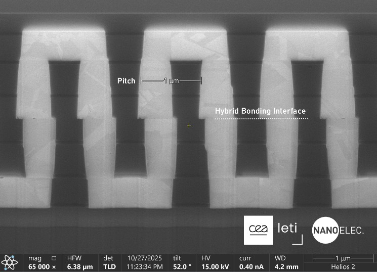
Photo: Cross-section of a 1µm-pitch D2W hybrid-bonded test vehicle
Achieving the 1 μm pitch required p...