Applied Materials, Inc. and SK hynix Inc. have entered a long-term collaboration agreement to develop next-generation DRAM and high-bandwidth memory (HBM) for AI and high-performance computing applications. The agreement establishes joint R&D programs focused on materials engineering, process integration, and 3D advanced packaging. Engineers from both companies will work side-by-side at Applied Materials’ EPIC Center in Silicon Valley as memory architectures move beyond current production nodes.
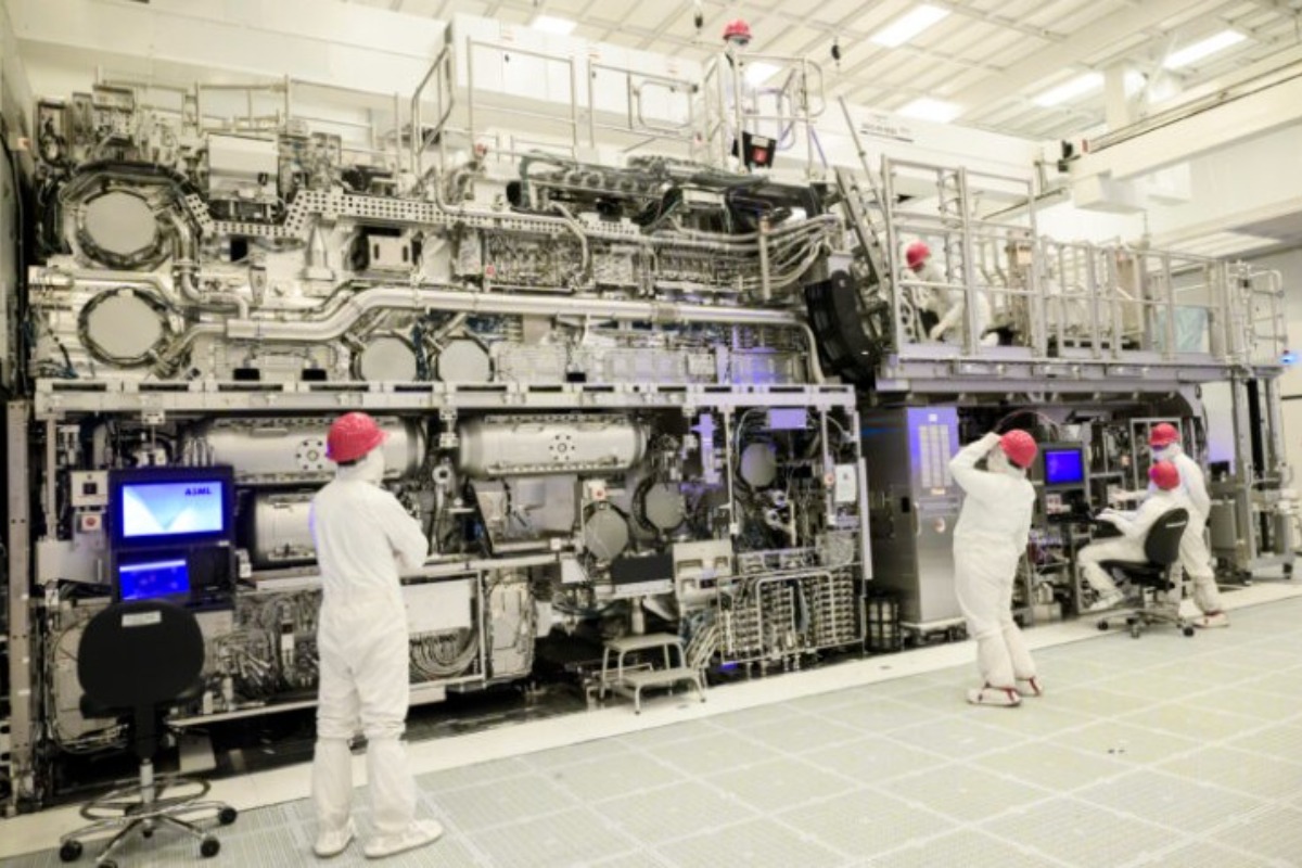
The EPIC (Equipment and Process Innovation and Commercialization) Center is scheduled to open this year. It is designed to give chipmakers and ecosystem partners earlier access to Applied Materials’ R&D portfolio, faster cycles of learning, and accelerated transfer of next-generation technologies into high-volume manufacturing. The facility represents Applied Materials’ planned investment of approximately $5 billion in advanced semiconductor equipment R&D in Silicon Valley, with capital spending expected to scale over time to that amount as customer projects commence. It is described as the largest-ever U.S. investment in this area.
Under the comprehensive technology development agreement, the initial co-innovation programs will explore new materials, complex integration schemes, and HBM-class advanced packaging to improve performance and manufacturability of future memory architectures. The work will use the EPIC Center’s high-velocity co-innovation model.

SK hynix will also utilize Applied Materials’ advanced packaging R&D capabilities in Singapore, linking device-level innovation with heterogeneous integration for 3D advanced packaging challenges.SK hynix becomes a founding partner of the EPIC Center. The companies have a prior history of joint work on energy-efficient performance of advanced memory chips through materials engineering innovations.
Statements from executives:
Gary Dickerson, President and CEO of Applied Materials: “Applied Materials and SK hynix share a long history of working together to improve the energy-efficient performance of advanced memory chips through innovations in materials engineering. We are excited to have SK hynix join the EPIC Center as a founding partner, and we look forward to driving further breakthroughs together that accelerate commercialization of next-generation DRAM and HBM technologies for the AI era.”
Nohjung Kwak, President and CEO of SK hynix: “The continued scaling of AI systems is driving unprecedented demand for energy-efficient memory technologies. One of the biggest hurdles in AI progress is the growing disconnect between memory speeds and advances in processors. Our advanced memory technologies are paving the way for faster and more energy-efficient data processing, and we look forward to partnering with Applied Materials at the new EPIC Center to deliver a roadmap of innovations that enable the next generation of memory solutions optimized for AI.”

Dr. Prabu Raja, President of the Semiconductor Products Group at Applied Materials: “Continued progress in memory increasingly relies on materials engineering innovations across both the device and packaging level. By combining the power of the EPIC Center in Silicon Valley with Applied’s advanced packaging capabilities in Singapore, our collaboration with SK hynix will enable us to co-optimize the entire technology stack and accelerate the path to manufacturable memory innovations.”
Seon Yong Cha, Chief Technology Officer of SK hynix: “Advancing memory technology for the AI era requires new approaches to developing wafer fab equipment. Our co-innovation programs with Applied Materials will focus on new materials, integration approaches and thermal-management technologies spanning device engineering and advanced packaging. Working alongside Applied engineers at the EPIC Center gives our teams faster learning cycles and manufacturing-relevant validation for next-generation AI memories.”
No additional details on timelines, specific technical targets, or financial terms of the agreement were disclosed in the announcement.