In the AI accelerated world of semiconductor chip design, ensuring the reliability and performance of increasingly complex chips is critical. Design for Test (DFT) technologies play a important role in this process, and few have shaped the field as profoundly as Janusz Rajski, a leading expert at Siemens Digital Industries Software. In an exclusive interview with me at the recently held semiconductor test event ITC India 2025 in Bangalore, Janusz Rajski, a pioneer in DFT and silicon lifecycle management after his keynote at the event, shared to me insights into transformative technologies like the Streaming Scan Network (SSN) and Tessent TestKompress, which are redefining how chips are tested and monitored throughout their lifecycle.
As chip designs grow exponentially in size and complexity doubling in data volume every two years, according to Janusz Rajski the need for scalable, efficient testing solutions has never been greater. “The challenges are very significant,” Rajski explains. “We need to understand not just current problems but also envisage future ones. That’s been the tradition of Siemens EDA’s R&D, which I’ve been proud to lead.”
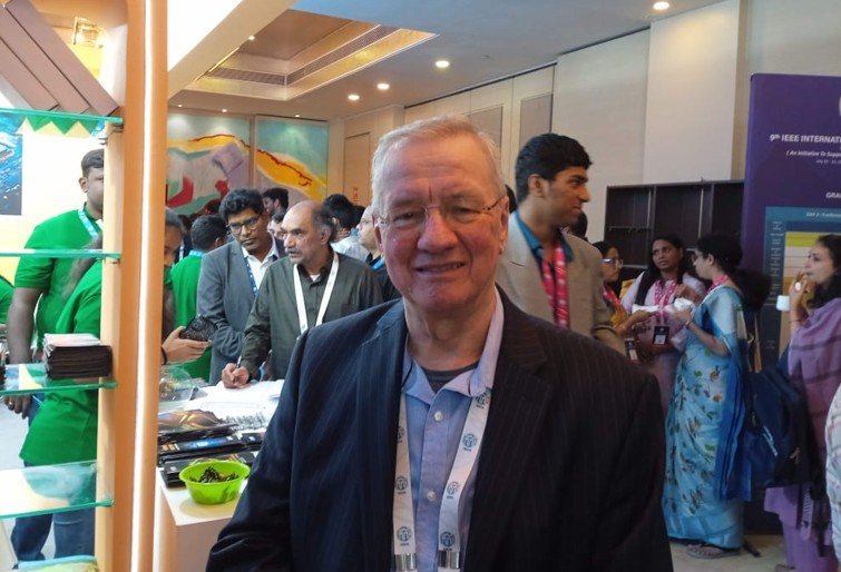
Pic: Janusz Rajski at the event
Rajski’s forward-thinking approach has driven the development of technologies that anticipate the industry’s needs. One such innovation is Tessent TestKompress, introduced in 2009, which achieves test compression ratios of up to 100x and is now a cornerstone of modern chip testing. “Pretty much every big design uses compression today,” Rajski notes, emphasizing its widespread adoption. The product, spelled with a distinctive “K” (TestKompress), has become synonymous with reducing test time and costs, enabling designers to tackle increasingly intricate chips.
The Streaming Scan Network: A Game-Changer for DFT: Streaming Scan Network (SSN) addresses the challenges of testing chips with hundreds of cores, some designs, Rajski notes, include up to 500 cores. “You don’t wait until you have the whole chip to generate test patterns,” he explains. “Core by core, designers can create patterns, and SSN automates the process of combining them into a single pattern for the entire chip.”

This “shift-left” approach drastically reduces test development time, which could otherwise take months for large designs. SSN also operates at high speeds, shifting data at up to 400 MHz, compared to the 100 MHz or less typically used for individual cores. “This makes the test application time much shorter,” Rajski says, a critical advantage as chip complexity grows.
Beyond testing, SSN’s versatility has made it a platform for broader applications. For instance, it enhances the iJTAG standard, traditionally limited to a single-wire, low-frequency interface. With SSN, designers can leverage a parallel bus of up to 72 or 100 lanes, achieving significantly higher throughput. “This is a very big improvement,” Rajski emphasizes, noting its ability to program cores and handle large volumes of test data efficiently.
Silicon Lifecycle Management: Testing Beyond Manufacturing: Rajski’s vision extends beyond traditional manufacturing tests to silicon lifecycle management (SLM), ensuring chips remain reliable throughout their operational life. Modern chips incorporate sensors like PVT (Process, Voltage, Temperature) monitors and slack sensors to track performance in real time. SSN enables the reading and integration of this sensor data, allowing periodic testing to assess whether a chip such as one in a server requires maintenance or replacement.
“This is not just about testing during manufacturing,” Rajski explains. “It’s about monitoring the chip’s health throughout its life.” This capability is increasingly vital as chips power critical applications in data centers, automotive systems, and AI-driven technologies.

Janusz Rajski’s contributions are backed by numerous patents and technical papers, underscoring the originality of his work. “SSN is unique in the market,” he asserts, highlighting its role as a patented technology that sets Siemens apart. His leadership in Siemens’ Tessent division has cemented its reputation as a leader in DFT, building on a legacy that began with Mentor Graphics (acquired by Siemens in 2017).
Reflecting on his work, Rajski emphasizes the importance of collaboration with customers. “We’ve found SSN to be a platform for many things,” he says, citing its adaptability to diverse testing needs. This customer-centric approach ensures that Siemens’ solutions remain aligned with the real-world challenges faced by chip designers.
As the semiconductor industry grapples with exponentially growing design complexity, innovators like Janusz Rajski are paving the way for the future. Technologies like Tessent TestKompress and SSN not only address today’s testing demands but also anticipate tomorrow’s challenges, ensuring chips are faster, more reliable, and sustainable throughout their lifecycle. For chip designers and the broader semiconductor ecosystem, Rajski’s work is a beacon of innovation, proving that even the most daunting challenges can be met with transformative solutions.
Author: Srinivasa Reddy N