

Atomic Layer Etching Breakthrough: APS Technology Targets 14 Ångstrom Semiconductor Nodes Without EUV
The semiconductor industry, driven by the demand for smaller, more efficient chips, has relied on extreme ultraviolet (EUV) lithography to scale down to 2-nanometer processes. However, the high cost and complexity of EUV equipment, costing hundreds of millions, have limited its profitability for some manufacturers. While TSMC has successfully generated revenue using EUV, Intel and Samsung face challenges securing enough high-end customers to offset their investments, risking significant financial losses.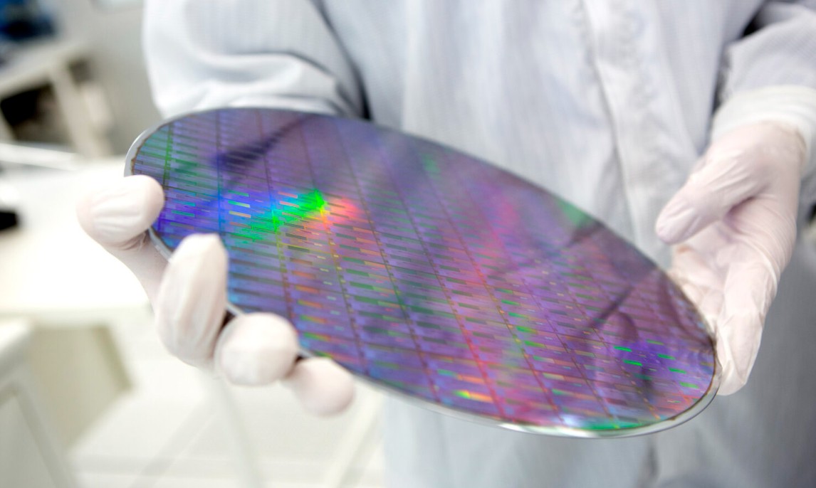
An European startup specializing in atomic layer etching (ALE) is developing a new approach called Atomic Layer Etch Pitch Splitting (APS). This nanostructuring technique, initially researched at Lund University, enables semiconductor patterning without EUV lithography. It splits nanoscale features into smaller structures using topographic selectivity and self-limiting chemical reactions, achieving critical dimensions below 10 nanometers and tight pitches on materials like silicon, dielectrics, and gallium phosphide (GaP).
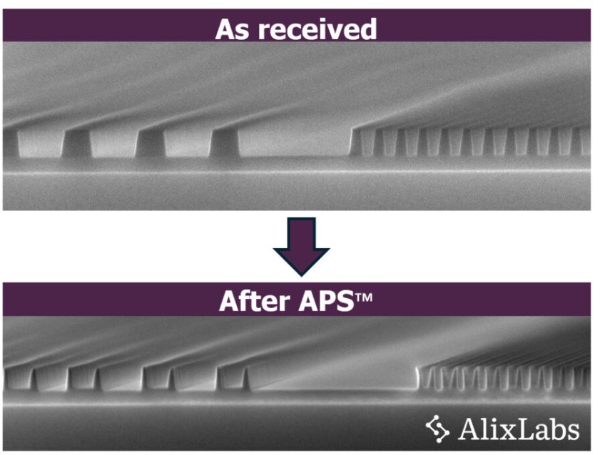
The APS process integrates with existing 300-millimeter logic and DRAM wafer production, as well as 150- and 200-millimeter wafers for gallium nitride (GaN) power ...
- Deep-technical articles & analysis
- New-product comparisons
- Premium online courses
- 1 author article / year