

Sub-2nm Semiconductor Manufacturing: Emerging Technologies for Sustainable, Cost-Effective Chip Production
Well, Many have concluded Moore's law has hit a wall a decade age, that's true to some extent but only in terms of the using Lithography tech used for decades from 1970s to 2020s. The totally new way of making nano devices are emerging using highly innovation techniques taking the integration and complexity further. The demand for sub-2nm node chipscritical for AI, quantum computing, and 5G/6G applications—has pushed the present well known extreme ultraviolet (EUV) lithography to its economic and environmental limits. With EUV systems costing upwards of $350 million and requiring immense energy, leading foundries like TSMC, Intel, and Samsung are grappling with profitability challenges, while the environmental footprint of complex multi-patterning processes grows. Fortunately, a wave of innovative technologies is emerging to address these issues, offering sustainable, cost-effective solutions for advanced chip manufacturing. Below explained are breakthroughs, spotlighting companies driving the charge toward sub-2nm nodes.
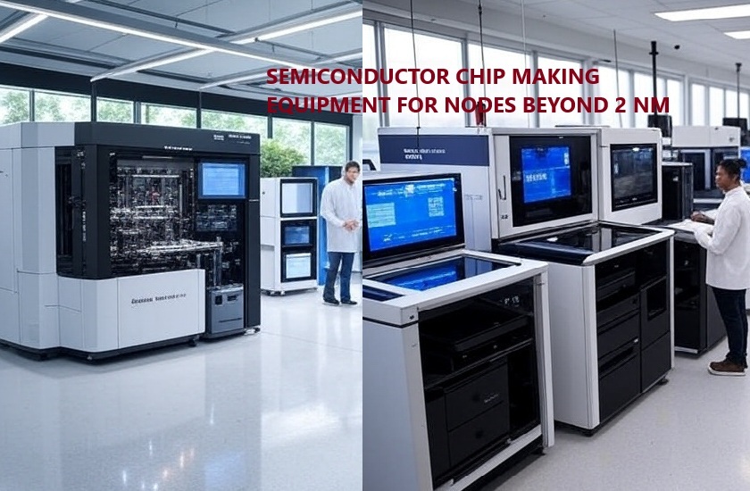
Atomic Layer Etching and Pitch Splitting: A Game-Changer for Precision and Sustainability
AlixLabs, a Swedish startup born from Lund University’s research, is redefining nanoscale patterning with its Atomic Layer Etch Pitch Splitting (APS) technol...
- Deep-technical articles & analysis
- New-product comparisons
- Premium online courses
- 1 author article / year