

Cleanroom in semiconductor manufacturing: Basic essential of a chip fab
Semiconductor cleanrooms are the backbone of modern chip production, creating controlled environments where the tiniest speck of dust can ruin intricate processes. These specialized facilities are essential for manufacturing, testing, and packaging semiconductor chips, which power everything from smartphones and household appliances to vehicles, defense systems, and spacecraft. The fragility of semiconductor materials, made from pure silicon wafers, demands rigorous standards to maintain their integrity and ensure the reliability of the devices they enable. Below, we explore the critical requirements for semiconductor cleanrooms, covering their classifications, design, equipment, and operational protocols.
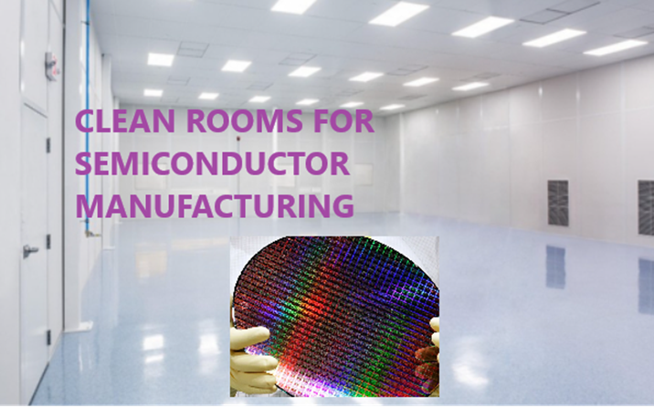
Stringent Cleanroom Classifications
Semiconductor cleanrooms operate under some of the strictest cle...
- Deep-technical articles & analysis
- New-product comparisons
- Premium online courses
- 1 author article / year