Japan based OKI is applying its Crystal Film Bonding (CFB) technology to fabricate chiplet based 3D IC heterogenous integrated devices particularly for analog semiconductor ICs. OKI's proprietary CFB technology lifts off the functional layer of a semiconductor device as a thin film and bonds it to a different material substrate using intermolecular forces without adhesives, allows for electrical, optical, and thermal propagation across the bond, enabling post-bonding semiconductor processes and the creation of new devices combining different materials and functionalities.
OKI says it has developed this technology as an alternate to the present 3D IC integration based on Through Silicon Vias (TSV), which as per OKI is a significant investment into equipment and advanced process development. Implementing the process using conventional technologies is claimed as expensive. OKI also able to cut the noise (crosstalk noise) generated by electrical signal interference. As we all know analog is a continuous signal rather than the logical signals in digital ICs, and handle higher voltage signals compared to digital ICs, making them more susceptible to crosstalk noise. Stacking ICs also increases the proximity between circuit layers, increasing crosstalk noise.
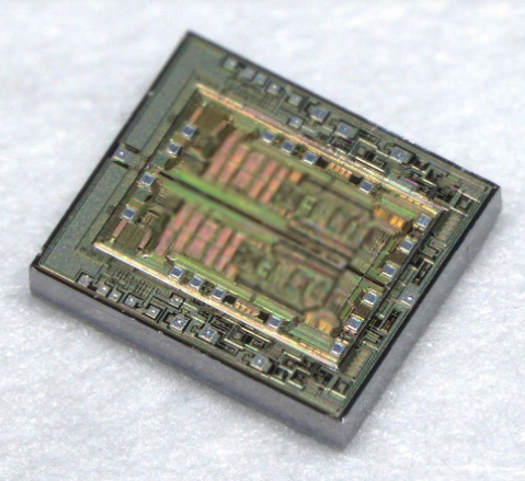
OKI has already producing CFB based integration of LEDs and ICs. OKI now has developed a new thin-film chiplet technology, consisting of lifting off thin film analog wafer and bonded to another thin film analog wafer/die, enabling the successful 3D integration of thin-film analog ICs. The size of bottom most wafer die is larger than the immediate next die to accommodate metal wiring pads exposed to final metal interconnecting.

OKI collaborated with Nisshinbo Micro Devices to achieve this 3D Integration of thin-film analog ICs using CFB technology. Nisshinbo Micro Devices has provided it proprietary shielding technology to shield each layer from the other. This shielding can be applied only to preferred areas.
However experts still cautious about this technology due to extreme thinness of wafers.

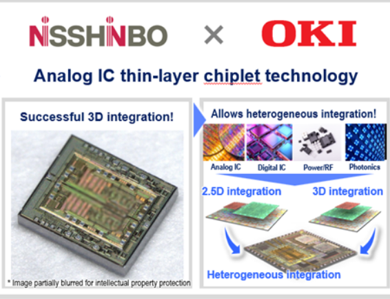
Both the companies have started developing new products based on this technology where they plan to mass produce by 2026.