Why lithography data preparation, process simulation, mask correction and metrology matter as much as the multi-million-dollar hardware, from research prototyping through to volume production
India is moving rapidly from semiconductor policy to physical infrastructure. As fabs, ATMP/OSAT facilities, research cleanrooms and prototype-fab initiatives take shape, another layer will determine how quickly these facilities can turn designs into repeatable devices, at any volume: the software and workflows between design, exposure and measurement.
India's semiconductor buildout is entering its execution phase
India's semiconductor story is no longer only about policy announcements. The country is now building physical capacity across manufacturing, packaging, research and the wider semiconductor supply chain.
The scale of the next stage is visible at SEMICON India 2026, which will bring more than 500 exhibiting companies to Yashobhoomi in New Delhi from 17 to 19 September. SEMI says the 2026 edition is focused on building a complete semiconductor ecosystem spanning design, manufacturing, packaging, equipment, materials, research, innovation and talent development.
That broader ecosystem matters because a semiconductor capability is not created by a fab alone. It depends on the ability to design, fabricate, measure, understand, improve and repeat reliably, at whatever volume the product demands.
India has made major progress on the hardware side. The Tata Electronics fab in Dholera, Micron's semiconductor assembly and test investment in Sanand, new ATMP/OSAT projects, and the expansion of research infrastructure all point toward a much deeper domestic semiconductor capability. SEMI has also reported that three of the 12 projects approved under the first phase of the Semicon India Programme have already commenced commercial production.
The next question is therefore not simply whether India can install more semiconductor equipment. It is whether the new facilities, from research cleanrooms up to high-volume fabs, can become productive, repeatable environments for device development, process development, mask making and manufacturing.
The missing layer between chip design and a fabricated device
India has built enormous strength in semiconductor design, EDA, verification and architecture. But there is a critical middle layer between a design file and a physical device, and it looks different depending on where a project sits on the path from first prototype to high-volume production.
At prototype and research scale, engineers need to fabricate a small number of devices, measure what was actually printed, understand the difference between intended and fabricated geometry, modify the process and run again. That cycle is the foundation of process development, and it is especially important for emerging technologies such as photonics, compound semiconductors, GaN, MEMS, quantum devices and neuromorphic hardware, which often require specialized lithography processes and rapid iteration.
At production scale, the same underlying questions apply to optical lithography on steppers and to the photomasks that drive them. A fab running 193nm, 248nm or 365nm exposure tools needs the printed pattern, and the mask that creates it, to match design intent run after run, wafer after wafer, not just once in a lab.
India's research ecosystem is already moving in this direction. CeNSE at IISc is developing INFIfab as a deep-tech translation centre, while IITs and other institutions are expanding cleanroom and nanofabrication capabilities. Programs such as INUP have also built a large academic user base and trained thousands of researchers. As Indian projects mature from these research environments toward pilot and volume manufacturing, the software layer has to scale with them.
As these facilities become operational, the practical question becomes: what happens to a design file after it leaves the CAD environment, and before the final device, or the mask that will print millions of them, is measured?
A GDS file does not become a device by itself
A layout represented in GDSII or OASIS is a description of the intended geometry. It is not automatically the geometry that will appear on a wafer, or on the photomask used to expose it.
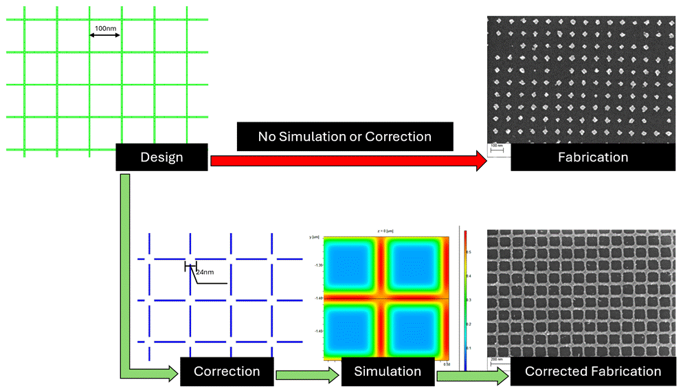
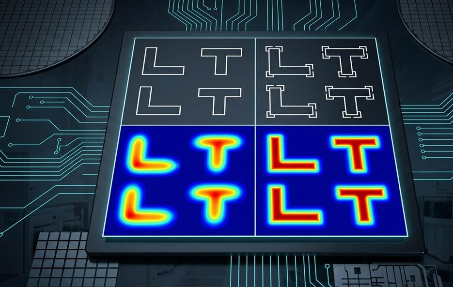
Before exposure, the layout has to be prepared for the specific lithography process and hardware. This may involve simulation, proximity-effect correction, optical proximity correction, process modelling, data conversion and fracturing.
For direct-write electron beam lithography, the proximity effect is a central challenge. Electrons scatter in the resist and substrate, depositing energy outside the intended feature. A line that is perfectly defined in the design database can therefore print wider or narrower than intended. Corners can round, isolated and dense features can behave differently, and nearby structures can influence one another. The solution is not simply to reduce or increase dose globally: a useful correction requires a physics-based understanding of how the process responds to different geometries and densities, so the layout can be modified before exposure and the printed result brought closer to design intent.
The same discipline is just as critical further down the production chain. 193nm, 248nm and 365nm optical steppers are the workhorse tools of mainstream, high-volume semiconductor manufacturing, and they face their own diffraction and process effects. Lithography process simulation and optical proximity correction (OPC) are what allow an engineer to reliably predict how a pattern will actually print on these steppers, and to correct the photomask itself before it goes into production, rather than discovering a systematic offset after thousands of wafers have already been exposed. Reliable mask correction at this stage is not a nice-to-have; it is what keeps a stepper-based process in specification across lots, tools and time.
This is the first invisible software layer in a fabrication workflow, and it applies whether the target is a handful of research devices or a mask set headed for volume production.

Metrology closes the loop
The second invisible layer appears after exposure and development. The key question is simple: did the pattern print as intended, on the wafer and on the mask?
In a production environment, critical dimensions and pattern characteristics are measured systematically using automated metrology. In many research environments, however, SEM measurements remain highly manual. An engineer may select a few images, measure a few lines and record the results by hand.
That approach can be enough to demonstrate that a process works. It is much less effective when the goal is to establish a repeatable process that can be transferred to another wafer, another researcher, another tool, another mask revision, or eventually an industrial partner.
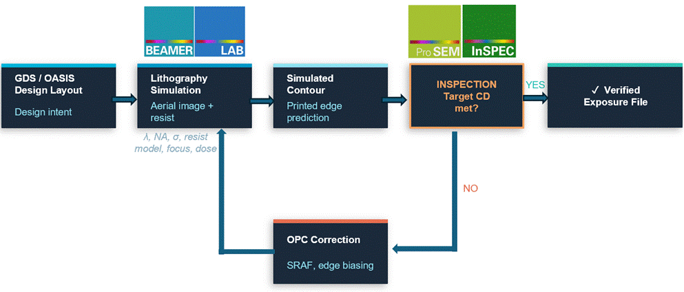
Automated SEM metrology changes the workflow. Instead of treating measurement as a final inspection step, the measurement data becomes part of process development. Critical dimensions, linewidths, shapes and other parameters can be extracted consistently and compared against the intended design. The result is a closed loop: design, simulate, correct, expose, measure, analyse and improve.
Why this matters across India's fabrication ambitions, prototype and production alike
A prototype foundry succeeds when it can offer more than access to equipment. It needs to offer predictable processes. A production fab succeeds on the same principle, at much larger scale and with far less tolerance for drift.
For a startup developing a photonic device, a university building a new MEMS structure, a research team working on GaN or quantum devices, or a fab running high-volume optical lithography on 193nm, 248nm or 365nm steppers, the value of the facility rests on the ability to move from an idea, or a mask revision, to a measured, repeatable device.
That requires three things working together. First, the lithography system, whether e-beam/laser direct writer or optical stepper, must receive the right data for the process and hardware. Second, the exposure must be supported by simulation and correction so that the printed pattern, and the mask that produced it, are as close as possible to design intent. Third, the resulting wafer must be measured in a systematic way so that the process can be understood quantitatively.
Without that software layer, a fab, research or production, can become highly dependent on individual operator experience. With it, process knowledge can be captured, compared and transferred. This distinction becomes increasingly important as India moves from academic demonstrations toward prototype production, mask making and full technology transfer.
The global nanofabrication and mask-making community has already solved much of this problem
The good news is that India does not have to invent these workflows from scratch.
GenISys has been developing lithography and metrology software since 2005, spanning the full path from e-beam prototyping to high-volume optical manufacturing. Its BEAMER platform supports e-beam data preparation and proximity-effect correction. LAB provides lithography process simulation and OPC for optical and laser lithography, including the 193nm, 248nm and 365nm stepper processes that underpin mainstream volume manufacturing, giving engineers a reliable, physics-based way to predict how a layout will print and to correct the mask before it is committed to production. MASKER handles mask data preparation for these photomasks. ProSEM provides automated SEM metrology, and InSPEC supports wafer-scale automated inspection.
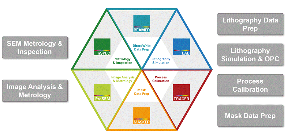
GenISys reports a global installed base of more than 1,300 licenses across academia, national laboratories and industries. Its users include leading universities, research laboratories and semiconductor and mask-making companies across North America, Europe and Asia, running everything from single-digit-nanometer research devices to production mask sets for high-volume fabs.
The company also operates as a hardware-agnostic software vendor, with integrations and partnerships spanning major lithography and inspection equipment manufacturers, from e-beam writers to optical steppers. That matters for emerging Indian facilities because the software layer should not force a research institution, or a production fab, to standardize on a single equipment supplier.
The important point is not any one software product. It is that the underlying workflows, for prototyping and for volume manufacturing alike, have already been developed, deployed and refined at hundreds of advanced nanofabrication facilities around the world.
India can therefore focus its engineering effort on developing the processes and devices that matter locally, rather than relearning every lesson about data preparation, proximity correction, mask correction and measurement from the beginning.
From equipment installation to process capability
The next phase of India's semiconductor journey will be measured by what the new infrastructure can actually produce.
Installing a lithography tool, e-beam writer or optical stepper, is an important milestone. Establishing a stable process window is more important. Being able to reproduce that process across wafers, masks, users and projects is what turns infrastructure into capability.

This is where software becomes part of the manufacturing and research infrastructure rather than an optional add-on. A modern fab workflow should make it possible to answer questions such as:
● How will this layout print before we expose it?
● What correction is required for this particular lithography process, on this particular tool?
● How sensitive is the pattern to dose, focus or process conditions?
● Did the fabricated feature, or the mask, match the intended critical dimension?
● How does the result vary across the wafer, or across a production lot?
● Can the process be transferred to another project, another user, or another tool?
The ability to answer those questions systematically is what converts a cleanroom or a fab, at any scale, into a learning and manufacturing platform.
The opportunity at SEMICON India 2026
India's semiconductor ecosystem is moving toward a more complete value chain. The next competitive advantage will come from how efficiently that ecosystem can convert equipment, engineering talent and research into repeatable technology, from first prototype to volume production.
That is why the software layer deserves more attention.
At SEMICON India 2026, GenISys will be showcasing its lithography data preparation, process simulation, proximity-effect correction, mask data preparation, SEM metrology and inspection solutions in Hall 2 at Booth H7509 at Yashobhoomi, New Delhi.
For teams building or operating semiconductor research and development infrastructure in India, at any scale, this is an opportunity to discuss a practical part of the workflow that is often overlooked: what happens between the design database and a measured, repeatable device or mask.
The semiconductor hardware investment is already underway. The next step is to make every new tool, wafer, mask and process run contribute more efficiently to India's growing pool of process knowledge.
The wheel has already been invented. India now has the opportunity to use it at scale.
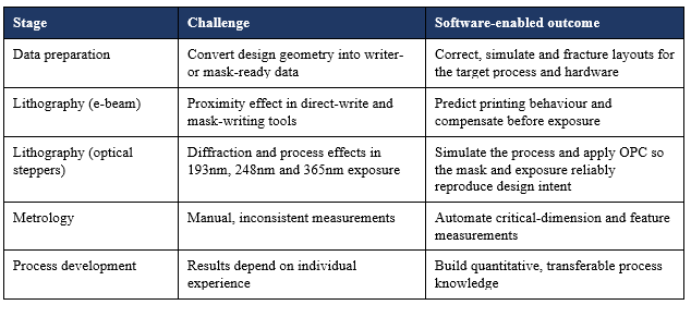
At a glance: where the software layer adds value
About GenISys
GenISys GmbH is headquartered in Munich, Germany. The company develops software for lithography data preparation, process simulation, proximity-effect correction, mask data preparation, SEM metrology and wafer-scale inspection, supporting workflows from e-beam research prototyping through high-volume 193nm, 248nm and 365nm optical manufacturing. Its BEAMER, LAB, MASKER, ProSEM and InSPEC platforms are used across academic, national-laboratory and industrial R&D and production environments worldwide. GenISys reports a combined installed base of more than 1,300 accounts.
Meet the GenISys team at SEMICON India 2026 • Booth H7509 • Yashobhoomi, New Delhi
www.genisys-gmbh.com | info@genisys-gmbh.com