

Advanced semiconductor package litho growing 18.6%, 4x faster than IC lithography
Sign in to read and print this article.
Semiconductor equipment market researcher Information Network finds advanced semiconductor package lithography growing 18.6%, 4x faster than IC lithography.
Lithography tools are used for patterning Advanced Packages such as fan-out wafer level packaging (FO-WLP), fan-in wafer level chip scale packaging (WLCSP), flip-chip and 2.5D/3D packaging that house leading edge Ics.
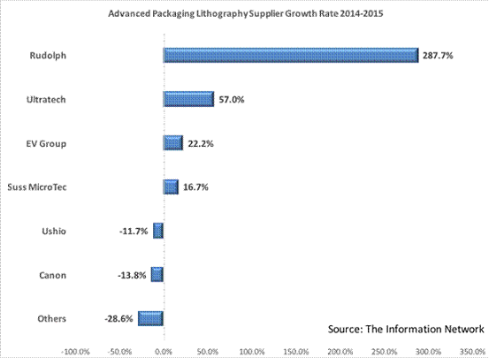
“The advanced package lithography sector was valued at $195 million, but is growing at four times the rate of mainstream IC lithography, 18.6% versus only 4.8%,” noted Dr. Robert Castellano, president of The Information Network. “Ultratech led the $195 million advanced packaging lithography market in 2015. Between 2014 and 2015, the company’s revenues grew 57.0%, but Rudolph Technologies’ revenues grew an astounding 287.7%.”
The report by Information Network details an analysis of the different types of steppers used in advanced packaging from each of the lithography suppliers listed in the chart below.
According to the report, advanced packaging lithography confronts a set of challenges that are unique to the application, meaning that an EUV or DUV mainstream lithography tool would not work. These include: • Feature sizes range from micrometers to hundreds of micrometers and oft...
According to the report, advanced packaging lithography confronts a set of challenges that are unique to the application, meaning that an EUV or DUV mainstream lithography tool would not work. These include: • Feature sizes range from micrometers to hundreds of micrometers and oft...
You've read this far — sign in to keep reading