

Sheet like insulation layer for semiconductor package substrates
Sign in to read and print this article.
To make the semiconductor chips used in smart phones further thinner, Panasonic has developed a sheet-form encapsulation material for coreless package substrates. The sheet-form encapsulation material which is scheduled for mass production from June 2016 is also reduces the cost making it suitable for large-area encapsulation.
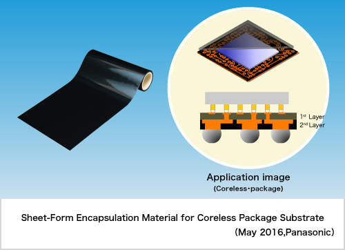
The new coreless process requires an insulation material for coreless processes that shows good productivity and eliminates the need for thin core materials as well as laser drilling processing. Panasonic used its resin design technology to develop a sheet-form encapsulation material for coreless package substrates. Panasonic shares below features of this semiconductor packaging material: A sheet-form encapsulation material with a uniformly produced insulation layer thickness is ideal for the new coreless process1, as it eliminates the need for laser drilling processing. The insulation layer for a package substrate can be produced using a large-area press process, enabling the mass production of packages at lower cost. - Sheet thickness is available in the range of 20 - 200 µm. The high rigidity of the thin sheet encapsulation material minimizes any warpage of packages and contributes to a thinner profile. Modulus of el...
The new coreless process requires an insulation material for coreless processes that shows good productivity and eliminates the need for thin core materials as well as laser drilling processing. Panasonic used its resin design technology to develop a sheet-form encapsulation material for coreless package substrates. Panasonic shares below features of this semiconductor packaging material: A sheet-form encapsulation material with a uniformly produced insulation layer thickness is ideal for the new coreless process1, as it eliminates the need for laser drilling processing. The insulation layer for a package substrate can be produced using a large-area press process, enabling the mass production of packages at lower cost. - Sheet thickness is available in the range of 20 - 200 µm. The high rigidity of the thin sheet encapsulation material minimizes any warpage of packages and contributes to a thinner profile. Modulus of el...
You've read this far — sign in to keep reading