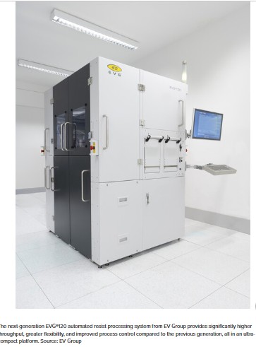
On February 18, 2026, EV Group (EVG), based in St. Florian, Austria, announced the introduction of the next-generation EVG120 automated resist processing system. This version updates an existing coater/developer platform by incorporating a compact architecture and features derived from the EVG150 system.
The system provides higher throughput, increased flexibility, and better process control than its predecessor, while occupying a reduced footprint suited to environments with diverse product mixes and resist processes.
It supports applications in advanced packaging, MEMS, image sensors, photonics, power devices, wafer probe cards, and related areas. The EVG120 handles spin coating, spray coating, and developing of photoresist materials for photolithography. It processes substrates from 2 inches to 200 mm and accommodates various resist types, such as thin and thick layers, positive and negative tone, dielectric materials including PI and PBO, and black/color/IR resists.

The redesigned platform uses a 200-mm configuration with up to two wet processing modules and 14 bake/chill plates, representing a 40% capacity increase over the prior version. The footprint is more than 20% smaller, with improvements for maintenance access and modular setup.
New features include:
Wafer Edge Exposure (WEE) for selective edge processing to achieve better edge accuracy and uniformity. In-situ resist thickness measurement for real-time monitoring, covering 50 nm to 50 microns, to support yield and control.
Enhanced high-viscosity dispense system with high-pressure delivery and closed-loop feedback for thick photoresists.
SMIF loadports for material handling.
Stand-by mode for lower energy use during idle times, compliant with SEMI E167.
The system retains existing technologies such as the CoverSpin bowl design for uniformity and reduced material use, and OmniSpray spray coating for conformal coverage on challenging topographies and fragile substrates.

Dr. Thomas Glinsner, corporate technology director at EV Group, stated that the platform draws on the company's experience in photoresist and lithography processing to address customer needs from R&D to volume production, combining performance, throughput, flexibility, and cost of ownership in a compact format.
EVG will present the EVG120 and related lithography solutions at the SPIE Advanced Lithography and Patterning Conference in San Jose, California, from February 22-26, 2026, at Booth #616. The company is also contributing technical papers to the program.
Orders for the next-generation EVG120 are now being accepted, with demonstrations available at EVG's headquarters. Further details are on the company's website at https://www.evgroup.com/products/lithography/resist-processing-systems/evg120.