Renesas Electronics has developed three System-on-Chip (SoC) technologies designed for automotive multi-domain electronic control units (ECUs). The technologies incorporate advanced AI processing and chiplet capabilities to serve as a platform for next-generation automotive electrical/electronic (E/E) architectures in software-defined vehicles (SDVs). The developments were presented at the International Solid-State Circuits Conference 2026 (ISSCC 2026), held February 15–19 in San Francisco.
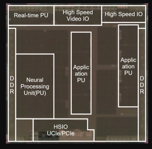
Automotive SoCs in the SDV era must support concurrent execution of multiple applications, enable scalability through chiplets, and satisfy functional safety standards. As multi-domain SoCs for central computing increase in size and complexity, preserving automotive-grade quality grows more challenging. Higher performance also drives up power consumption, necessitating gains in power efficiency and safety.

The three technologies address these requirements as follows:
1. Chiplet architecture supporting ASIL D functional safety. It integrates the standard UCIe die-to-die interface with a proprietary RegionID mechanism to prevent hardware resource interference during simultaneous application execution, ensuring Freedom from Interference (FFI). RegionIDs are mapped to physical address space, encoded into the UCIe region, and transmitted between dies functionality absent in conventional UCIe interfaces. This allows safe access control via the memory management unit (MMU) and real-time cores. Testing showed the UCIe interface maintains processor-to-memory bus bandwidth while achieving 51.2 GB/s transmission speed, close to intra-SoC transfer limits.

2. 3 nm SoC design enhancing neural processing unit (NPU) performance for AI while retaining automotive-grade quality. NPU area has increased 1.5-fold over previous generations, causing higher clock latency from shared clock sources to individual circuits. The design replaces module-level clock pulse generators (CPGs) with mini-CPGs (mCPGs) at the sub-module level to reduce latency and meet timing constraints. To handle test clock synchronization in the hierarchical structure—required for zero-defect quality in automotive use test circuits are integrated, user and test clock paths are unified, and upper- and lower-level mCPGs synchronize under a single clock source in test mode for unified phase adjustment.
3. Power gating technology with over 90 power domains for precise control ranging from milliwatts to tens of watts based on operating conditions. Power switches (PSWs) are divided into ring PSWs, which suppress rush currents during power-on, and row PSWs, which equalize impedance within domains, reducing IR drops by approximately 13% compared with conventional designs amid rising current density in smaller geometries. For ASIL D compliance, dual core lock step (DCLS) employs independent PSWs and controllers for master and checker cores to detect failures via lockstep operation. Loopback monitoring verifies each PSW gate signal to detect OFF-state failures. Voltage monitoring uses a digital voltage meter (DVMON) resistant to temperature drift, improving aging tolerance by 1.4 mV.
These technologies are implemented in the R-Car X5H SoC for automotive multi-domain ECUs, supporting SDV development with safety provisions for applications including autonomous driving and digital cockpits