The evolving role of TCAD in semiconductor design and manufacturing: From atoms to systems
Technology Computer-Aided Design (TCAD) has transcended its origins as a niche simulation tool to become an indispensable pillar of modern semiconductor development and manufacturing. As transistor dimensions shrink toward atomic scales and system complexity skyrockets, TCAD bridges the gap between fundamental physics and industrial production. This article examines TCAD’s critical current roles, its integration into manufacturing workflows, and its expanding future in an era defined by heterogeneous integration and design-technology co-optimization (DTCO).
TCAD Today: Multi-Scale Simulation for Complex Challenges
Contemporary TCAD tackles problems spanning nearly ten orders of magnitude:
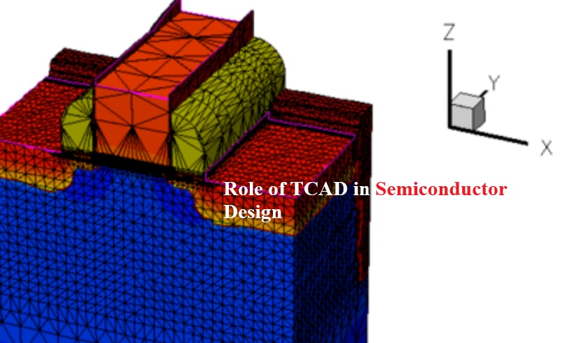
Atomic-Scale Modeling: Quantum effects are the most important for sub-10nm nodes like FinFETs and GAA Nanowires. To model carrier transport, bandstructure, and atomic-level defects (e.g., Ge nanowire leakage mechanisms like Band-to-Band Induced Barrier Lowering - BIBL), industrial TCAD departments often use strict methods like Non-Equilibrium Green's Function (NEGF) and Density Functional Theory (DFT) [1]. These simulations help make faster continuum models that are used in production.
Device and Process Simulation: Continuum models grou...