

Preventing Floor Vibration Impact on Nanometer-Scale Semiconductor Fabrication Facilities
Even a single hard footstep or the passage of a heavy truck near an advanced semiconductor fab can critically impair ongoing nanolithography and metrology processes if effective vibration isolation is not implemented. The precision required to fabricate chips at nanometer and sub-nanometer nodes is extraordinary: features are now comparable in size to individual atoms. In semiconductor fabs producing at these scales, floor vibration disrupts critical steps such as lithography patterning and e-beam metrology inspection, leading to misalignment, defects, and reduced yield.
In semiconductor fabs producing at nanometer nodes, floor vibration disrupts precision processes such as nanolithography patterning and e-beam metrology inspection, leading to pattern misalignment, defects, and reduced yield. Tools for lithography (wafer and mask patterning) and metrology (wafer inspection, defect review, failure analysis) require extremely low vibration levels. Urban fab sites expose facilities to external sources—road traffic, trucks, subways, trains, construction, wind, and acoustic noise and internal sources footfall, elevators, HVAC ducts, air compressors, pumps, and other machinery that drive floor motion, particularly near 2 Hz.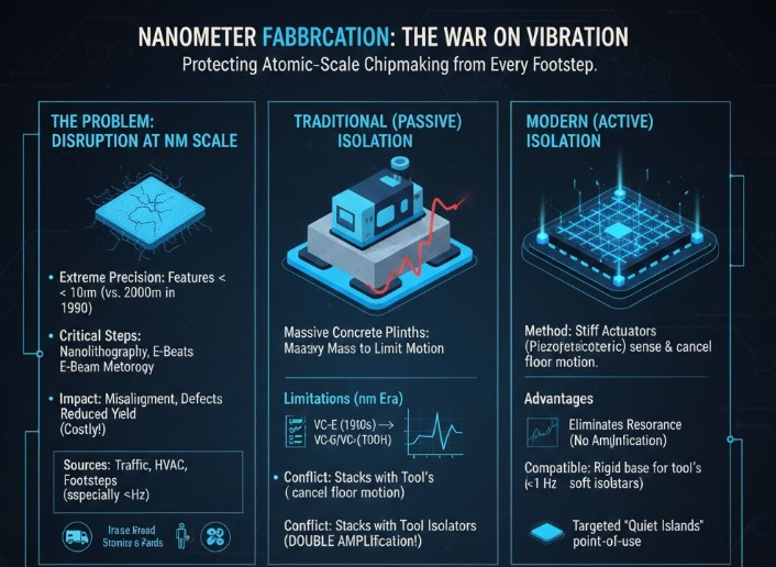
Tr...
- Deep-technical articles & analysis
- New-product comparisons
- Premium online courses
- 1 author article / year