

OKI Develops High-Accuracy Simulation Technology for High-Frequency Vias in 1.6 Tbps AI Data Center PCBs
OKI Circuit Technology (OTC), the OKI Group’s printed circuit board business company based in Tsuruoka City, Yamagata Prefecture, has developed High-Accuracy Simulation Technology for High-Frequency Vias. The technology enables precise control of via characteristics in multilayer PCBs designed for 1.6 Tbps-class high-speed transmission required by next-generation AI data centers.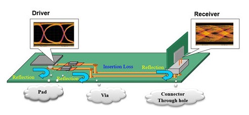
Issues with high-speed transmission PCBs
As generative AI systems expand, AI servers, data centers, and related semiconductors demand greater capacity and speed. This has led to increasingly multilayered and structurally complex PCBs, where reducing transmission losses and signal reflections is critical. Vias, the interlayer connection structures in multilayer PCBs, significantly affect high-frequency signals, making accurate control of via characteristic impedance essential to minimize signal reflection.
In high-frequency bands where the fundamental frequency exceeds 50 GHz, conventional via modeling methods have difficulty accurately reflecting manufacturing process effects, variations, and material properties in high-frequency regions. This has resulted in poor correlation between simulation results and actual measured characteristics, complicati...