

Ways to achieve both thermal and electrical performance in semiconductor packaging
Achieving high thermal and electrical performance in semiconductor packaging is critical for ensuring efficient power delivery, signal integrity, and heat dissipation in modern integrated circuits (ICs). Semiconductor packaging must address challenges like high power densities, miniaturization, and reliability in advanced nodes (e.g., 3 nm, 5 nm). Semiconductor devices generate heat during operation, and effective packaging is essential for dissipating this heat away from the sensitive die, with thermal resistance (θ) serving as a key metric to characterize a package's ability to conduct heat lower thermal resistance indicates better heat dissipation, with common metrics including θJA (junction-to-ambient), θJC (junction-to-case), and θJB (junction-to-board).
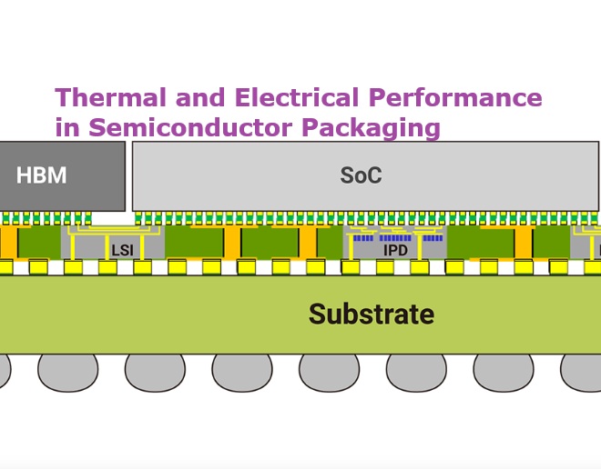
Below are key strategies to optimize both thermal and electrical performance in semiconductor packaging, presented concisely and comprehensively:
Advanced Packaging Materials:
High-Conductivity Substrates: Use substrates with high electrical and thermal conductivity, such as copper-clad laminates or silicon interposers, to enhance power delivery and heat dissipation.
Thermal Interface Materials (TIMs): Employ advanced TIMs (e.g., indium-based solders, graphene-enhanced pastes, or liquid m...
- Deep-technical articles & analysis
- New-product comparisons
- Premium online courses
- 1 author article / year