Wire bonding dominates semiconductor packaging amid emerge of new tech: Market, trends, and applications
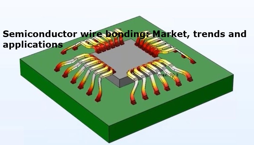
Wire bonding remains the dominant method for connecting semiconductor dies to circuit boards, accounting for 75-80% of first-level interconnections in microelectronics. This process uses fine metal wires such as gold, aluminum, copper, or gold-palladium plated copper to link bonding pads on a silicon die to a leadframe or package terminals, often enhanced by a silver-based functional film for improved conductivity. The wire bonding equipment market, valued at $800 million in 2022, is projected to reach $1.6 billion by 2030, driven by demand for advanced packaging and wide-bandgap semiconductors like silicon carbide and gallium nitride.
Wire bonding is widely used in consumer electronics, automotive microcontrollers, power ICs, analog, RF, mixed-signal chips, and legacy industrial systems. Its advantages include cost-effectiveness for low- to medium-volume production, a mature process, flexibility for various chip layouts, and micron-level precision. However, it faces limitations in high-speed, high-bandwidth applications due to higher parasitics, slower processing compared to flip-chip or through-silicon vias, and mechanical vulnerabilities to vibration or thermal stress.
The global bonding wires market is expected to grow significantly, with estimates projecting a market...
- Deep-technical articles & analysis
- New-product comparisons
- Premium online courses
- 1 author article / year