

Civil engineering challenges in building semiconductor fabrication facilities
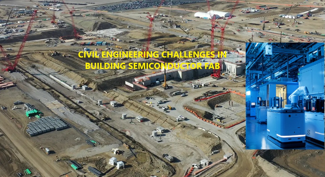
Semiconductor fabrication facilities (fabs) are among the most advanced structures in modern engineering, requiring extreme precision to produce microchips with nanometer-scale features. These facilities demand ultra-clean, vibration-free, and seismically resilient environments while mitigating risks from radiation and natural disturbances. Civil engineers face unique challenges in designing and constructing/building fabs to meet these stringent requirements. This article explores key challenges vibration control, shock mitigation, radiation protection, earthquake resilience, and other natural disturbances—and highlights innovative construction technologies, such as TMC’s Quiet Island system and other industry-leading solutions. Top construction companies and other experts are listed with analysis on their capabilities.
1. Vibration Control: Ensuring Nanometer-Scale Precision
Semiconductor manufacturing relies on equipment like photolithography machines, which require near-zero vibration tolerance. External sources (e.g., traffic, railways) and internal sources (e.g., HVAC systems, pumps) can disrupt processes, leading to defective chips. Raised fa...
- Deep-technical articles & analysis
- New-product comparisons
- Premium online courses
- 1 author article / year