

3D stacking of an AlGaN/GaN/Si HEMT on CPW lines fabricated on 200mm
Sign in to read and print this article.
CEA-Leti scientists presented three papers at the IEEE Symposium on VLSI Technology and Circuits detailing the institute's progress on 3D integration technologies, which are a promising approach for designing More than Moore systems, especially radio frequency (RF) integrated systems.
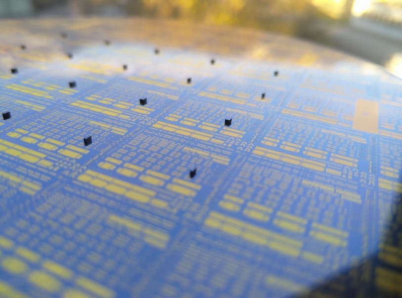
3D integration techniques enable high-density CMOS transistors to coexist with transistors made of III-V materials, which can reach power levels and frequencies unattainable with conventional silicon technologies. Potential applications include communications, the internet of things, medical devices and automotive sensing. 'RF Performances Are Competitive with Other 3D Solutions' The paper, “Hybrid Integration of 3D-RF Interconnects on AlGaN/GaN/Si HEMT RF Transistor featuring 2.2W/mm Psat & 41% PAE @28GHz using a Robust and Cost-Effective Chiplet Heterogeneous Bonding Technique", reports the stacking of an AlGaN/GaN/Si high electron mobility transistor (HEMT) on coplanar-waveguide (CPW) lines fabricated on 200mm silicon trap-rich substrate. The HEMT and CPWs lines were interconnected with copper pillars (CuPi) using a high-yield chiplet heterogeneous integration process. “Thanks to the integration of low insertion loss CuPi interconnects – 0.1dB@28GHz and a careful management of the heat dissipation wit...
3D integration techniques enable high-density CMOS transistors to coexist with transistors made of III-V materials, which can reach power levels and frequencies unattainable with conventional silicon technologies. Potential applications include communications, the internet of things, medical devices and automotive sensing. 'RF Performances Are Competitive with Other 3D Solutions' The paper, “Hybrid Integration of 3D-RF Interconnects on AlGaN/GaN/Si HEMT RF Transistor featuring 2.2W/mm Psat & 41% PAE @28GHz using a Robust and Cost-Effective Chiplet Heterogeneous Bonding Technique", reports the stacking of an AlGaN/GaN/Si high electron mobility transistor (HEMT) on coplanar-waveguide (CPW) lines fabricated on 200mm silicon trap-rich substrate. The HEMT and CPWs lines were interconnected with copper pillars (CuPi) using a high-yield chiplet heterogeneous integration process. “Thanks to the integration of low insertion loss CuPi interconnects – 0.1dB@28GHz and a careful management of the heat dissipation wit...
You've read this far — sign in to keep reading