

Atomic level semiconductor chip making at <7 nm, Indian engineers are playing
Sign in to read and print this article.
"Raw talent is exist no matter what you do with that person" quotes Krishnan Srinivasan, Managing Director of the fast growing semiconductor fab-rication equipment maker Lam Research India, when this writer asked about India engineering is not only about IITs.
Lets talk about 6 nm width transistor, it has just 30 silicon atoms. So if you are a semiconductor equipment designer, you need to design your equipment to alter the silicon or some other semiconductor material using some atomic level altering material processing machines.
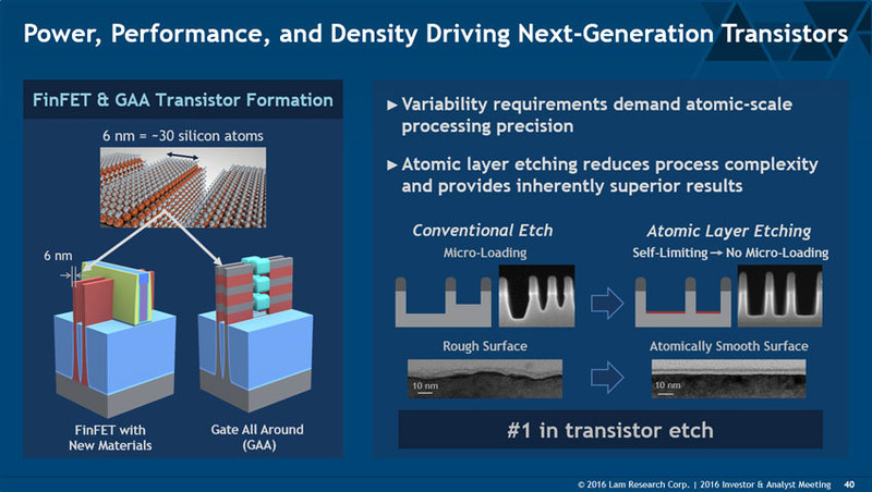
Pic above: Atomic scale structure of FinFETs and the etching Lam Research success in India speaks about availability of semiconductor equipment talent for deep node chip equipment development. In an exclusive interaction at Lam Research India office in Bengaluru, K. Srinivasan explained to this writer, the technology and business connections driving the high end semiconductor fab-rication technology. K. Srinivasan: The most fundamental macro-economic trend what we call knowledge economy, which to me represents development of generation of knowledge. If you look at that- then you can narrow down, that drives our system integrators to develop products and today the main thrust is on enterprise computing. With that you also have mobility re...
Pic above: Atomic scale structure of FinFETs and the etching Lam Research success in India speaks about availability of semiconductor equipment talent for deep node chip equipment development. In an exclusive interaction at Lam Research India office in Bengaluru, K. Srinivasan explained to this writer, the technology and business connections driving the high end semiconductor fab-rication technology. K. Srinivasan: The most fundamental macro-economic trend what we call knowledge economy, which to me represents development of generation of knowledge. If you look at that- then you can narrow down, that drives our system integrators to develop products and today the main thrust is on enterprise computing. With that you also have mobility re...
You've read this far — sign in to keep reading