
FDSOI; The only semiconductor tech to continue Moore's Law down to 10nm
While the semiconductor fab industry facing big hurdle in scaling further down after 28nm without increase in cost, blessing for the industry comes in the form of new technology called fully depleted silicon-on-insulator (FDSOI). FDSOI can take Moores law down to 10nm. STMicroelectronics is already making 28nm chips out of its Crolles, France fab using FDSOI, ST and its partners have also licensed FDSOI tech to leading foundry Samsung to produce 28nm chips using FDSOI. Below is the Q & A interaction with ST's Rajamohan Varambally, Director, Central CAD and design solutions, STMicroelectronics India.
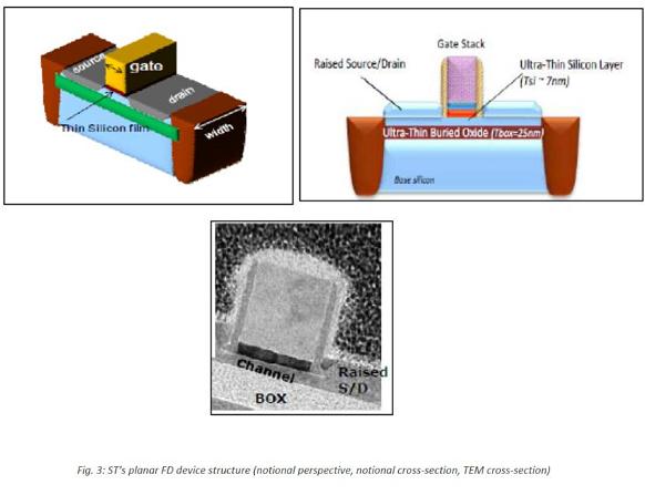
Q. What is FD-SOI?
FD-SOI stands for Fully Depleted Silicon On Insulator. Planar fully depleted silicon-on-insulator (“planar FD”, or equivalently “FD-SOI”) transistors are planar CMOS transistorsfabricated in a very thin layer of silicon sitting over a layer of buried oxide (BOX). They are therefore ‘ultra-thin body’ (UTB) devices: the electrical conduction channel that forms between source and drain is confined to this ultra-thin silicon layer under the gate oxide.
Q. What makes this process better than other deep-node semiconductor chip fabrication tech? 1. Immunity to Short-Channel Effects Ultra-thin body and BOX ensures all electrical paths between s...
Q. What makes this process better than other deep-node semiconductor chip fabrication tech? 1. Immunity to Short-Channel Effects Ultra-thin body and BOX ensures all electrical paths between s...
You've read this far — sign in to keep reading