Nikon Introduces DSP-100 Digital Lithography System with Large 600x600mm Wafer Support for Semiconductor Packaging in 2025
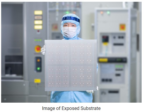
Nikon Corporation said it will start accepting orders for its Digital Lithography System DSP-100, tailored for back-end semiconductor manufacturing, in July 2025, with a scheduled release in Fiscal Year 2026. The system targets advanced packaging applications, supporting square substrates up to 600x600mm and achieving a resolution of 1.0μm (Line and Space).
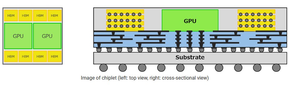
The DSP-100 addresses the rising demand for high-performance semiconductor devices driven by high-speed communication technologies, such as IoT and generative AI, particularly in data centers. It supports advanced packaging methods like chiplets, which connect multiple chips side by side, and panel-level packaging (PLP) using resin or glass substrates, as circuit patterns become finer and package sizes increase.
Key features include a resolution of 1.0μm L/S, an i-line equivalent light source, and an overlay accuracy of ≤±0.3μm. The system supports substrates up to 600x600mm, including wafers, and achieves a throughput of 50 panels per hour on 510x515mm substrates. It integrates Nikon’s semiconductor lithography tech...