World's first equipment to modify semiconductor material properties
Japan-based semiconductor equipment manufacturer Nissin Ion Equipment has announced the development of a semiconductor equipment/machine for modifying semiconductor material such as silicon to have properties which were not present in the original material. By changing the properties of materials and improving the functionality of material, it helps in improving the device performance and also supporting advanced manufacturing technology.
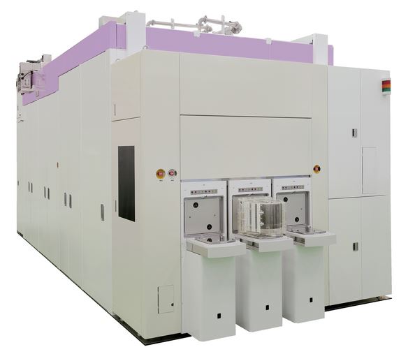
The equipment is named as KYOKA, can handle mass production of such material modification processes aligning with the today's advanced semiconductor manufacturing equipments producing highly advanced chips for AI applications. By using high current ion technology which is developed for the smartphone display manufacturing, this equipment handles high throughput at low processing cost. Nissin Ion Equipment plans to install a demonstration system at its Shiga plant as a trial for its customers. The new equipment uses extreme large volume of ions compared to conventional equipment. KYOKA can handle 25 wafers and more per hour. KYOKA can also support low-energy regions under 1keV through the use of ultra-high current ion beams. This equipment provides option to generate variety of ion species to achieve optimal modification in accordance with...
The equipment is named as KYOKA, can handle mass production of such material modification processes aligning with the today's advanced semiconductor manufacturing equipments producing highly advanced chips for AI applications. By using high current ion technology which is developed for the smartphone display manufacturing, this equipment handles high throughput at low processing cost. Nissin Ion Equipment plans to install a demonstration system at its Shiga plant as a trial for its customers. The new equipment uses extreme large volume of ions compared to conventional equipment. KYOKA can handle 25 wafers and more per hour. KYOKA can also support low-energy regions under 1keV through the use of ultra-high current ion beams. This equipment provides option to generate variety of ion species to achieve optimal modification in accordance with...
You've read this far — sign in to keep reading